
Mobile Intel Pentium 4 Processor - M and Intel 845MP/MZ Chipset Platform Design Guide

Mobile Intel
®
Pentium
®
4 Processor-M and Intel
®
845MP/845MZ Chipset Platform
Design Guide 77
R
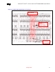
5.2.4. Clock Signals – SCK[5:0], SCK#[5:0]
The clock signal group includes the differential clock pairs SCK[5:0] and SCK#[5:0]. The MCH-M
generates and drives these differential clock signals required by the DDR interface; therefore, no external
clock driver is required for the DDR interface. The MCH-M only supports unbuffered DDR SO-
DIMMs, three differential clock pairs are routed to each SO-DIMM connector. Table 20 summarizes the
clock signal mapping.
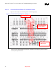
Table 20. Clock Signal Mapping
Signal Relative To
SCK[2:0], SCK#[2:0] SO-DIMM0
SCK[5:3], SCK#[5:3] SO-DIMM1
Note: One to one mapping of the clocks from the MCH-M to the SO-DIMM is not required. For example, it is
not necessary that SCK0 from the MCH-M routes to the same number clock on the SO-DIMM0
connector, which is CK0 in the PC2100 and PC1600 DDR SDRAM Unbuffered SO-DIMM Reference
Design Specification. However CKn and CKn# may not be swapped from the MCH-M to the SO-
DIMMs. The changing of clock numbering from MCH-M to SO-DIMMs may require a BIOS change.
The clock signal routing
should transition from an external layer to an internal signal layer under the
MCH-M and route as a differential pair referenced to ground for the entire length to their associated SO-
DIMM connector pads. Immediately prior to the SO-DIMM connector the signals should transition to an
external layer to connect the appropriate pad of the connector.
External trace lengths should be minimized. All internal and external signal routing should be ground
referenced to keep the path of the return current continuous.
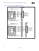
The diagrams and table below depict the recommended topology and layout routing guidelines for the
DDR-SDRAM differential clocks.
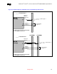
Figure 36. DDR Clock Routing Topology (SCK/SCK#[2:0])
SO-DIMM0,1 PAD
MCH-M
Pad
MCH-M Package
L1