
Mobile Intel Pentium 4 Processor - M and Intel 845MP/MZ Chipset Platform Design Guide

Mobile Intel
®
Pentium
®
4 Processor-M and Intel
®
845MP/845MZ Chipset Platform
78 Design Guide
R
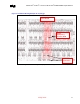
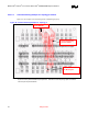
Table 21. Clock Signal Group Routing Guidelines
1
Parameter Routing Guidelines Figure
Signal Group Clock – SCK[5:0], SCK#[5:0]
Topology Differential Pair Point to Point Figure 35
Reference Plane Ground Referenced
2
Characteristic Trace Impedance (Zo) Single Ended =55 Ω ± 15%
Trace Width Inner layers= 4 mils
Outer layer= 5 mils
Differential Trace Spacing Inner layers= 4 mils
Outer layer= 5 mils
Group Spacing Isolation spacing from another DDR signal group =
20 mils
Isolation spacing from non-DDR related signals =
20 mils
Serpentine Spacing 12 mils minimum
Trace Length L1 – MCH-M Signal ball to
Associated SO-DIMM0 Connector Pad
Min = 1.5”
Max= 8.0”
Figure 35
Maximum Recommended motherboard via
Count per signal
2 vias
Length Matching Requirements SCK / SCK#
The three SO-DIMM0 Clock pairs are equal in
length plus tolerance, and the three SO-DIMM1
Clock pairs are equal in length plus tolerance.
See Section 5.2.4.1 for details
Figure 38,
Figure 39
Clock pair to pair tolerance ± 25 mils
SCK to SCK# tolerance ± 10 mils
NOTES:
1. Recommendation may change in a later revision of the design guide based on a post silicon simulation
analysis.
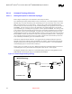
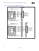
2. Wherever possible the clock signals should be routed on adjacent layers to the referenced ground plane. See
Figure 37 for example. The clock signal routing should only route on Signal 1 and Signal 2 layer where Signal 1
may be external (microstrip) and Signal 2 may be internal (stripline) or where Signal 1 is internal (stripline) and
Signal 2 is external (microstrip).
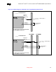
Figure 37. Ground Referencing Plane Stack-up