
Mobile Intel Pentium 4 Processor - M and Intel 845MP/MZ Chipset Platform Design Guide

Mobile Intel
®
Pentium
®
4 Processor-M and Intel
®
845MP/845MZ Chipset Platform
Design Guide 81
R
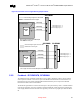
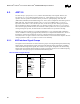
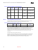
Figure 39. Clock Pair Trace Length Matching Requirements
SO-DIMM0
MCH-M Package
MCH-M
DIE
= MCH Package Lengths from Pad to Ball
= Motherboard Trace Lengths
Note: Lengths are measured from MCH-M pad
to SO-DIMM0 connector pins
SCK/SCK#[0]
SCK/SCK#[1]
SCK/SCK#[2]
SCK/SCK#[0] Length = X
SCK/SCK#[1] Length = X
SCK/SCK#[2] Length = X
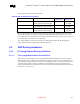
SO-DIMM0
SO-DIMM1
MCH-M Package
MCH-M
DIE
SCK/SCK#[3]
SCK/SCK#[4]
SCK/SCK#[5]
Note: Lengths are measured from MCH-M pad to SO-DIMM1 connector pins
SCK/SCK#[5] Length = Y
SCK/SCK#[3] Length = Y
SCK/SCK#[4] Length = Y
= MCH-M Package Lengths from Pad to Ball
= Motherboard Trace Lengths
5.2.5. Feedback - RCVENOUT#, RCVENIN#
The MCH-M provides a feedback signal called “receive enable” (RCVEN#), which is used to gate the
strobe inputs for read data. There are two pins on the MCH-M to facilitate the use of RCVEN#. The
RCVENOUT# pin is an output of the MCH-M and the RCVENIN# pin is an input to the MCH-M.
RCVENOUT# must connect to RCVENIN#.
The RCVEN# signal must be routed on the same layer as the system memory clocks. It should transition
from the top signal layer to an inner signal layer under the MCH-M, routed referenced to ground for the
entire length, and then transition from the inner signal layer back to the top signal layer under the MCH-
M.