
Mobile Intel Pentium 4 Processor - M and Intel 845MP/MZ Chipset Platform Design Guide

Mobile Intel
®
Pentium
®
4 Processor-M and Intel
®
845MP/845MZ Chipset Platform
86 Design Guide
R
6.2. AGP 2.0
The AGP Interface Specification, rev. 2.0, enhances the functionality of the original AGP Interface
Specification
(rev. 1.0) by allowing 4X data transfers (i.e., 4 data samples per clock) and 1.5-volt
operation. The 4X operation of the AGP interface provides for "quad-pumping" of the AGP AD
(address/data) and SBA (side-band addressing) buses. That is, data is sampled four times during each 66-
MHz AGP clock. This means that each data cycle is ¼ of a 15-ns (66-MHz) clock or 3.75 ns. It is
important to realize that 3.75 ns is the data cycle time, not the clock cycle time. During 2X operation,
data is sampled twice during a 66-MHz clock cycle; therefore, the data cycle time is 7.5 ns. In order to
allow for these high-speed data transfers, the 2X mode of AGP operation uses source-synchronous data
strobing. During 4X operation, the AGP interface uses differential source-synchronous strobing.
With data cycle times as small as 3.75 ns and setup/hold times of 1 ns, propagation delay mismatch is
critical. In addition to reducing propagation delay mismatch, it is important to minimize noise. Noise on
the data lines will cause the settling time to be long. If the mismatch between a data line and the
associated strobe is too great or if there is noise on the interface, incorrect data will be sampled. The low-
voltage operation on AGP (1.5 V) requires even more noise immunity.
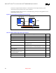
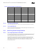
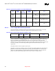
6.2.1. AGP Interface Signal Groups
The signals on the AGP interface are broken into three groups: 1X timing domain signals, 2X/4X timing
domain signals, and miscellaneous signals. Each group has different routing requirements. In addition,
within the 2X/4X timing domain signals, there are three sets of signals. All signals in the 2X/4X timing
domain must meet minimum and maximum trace length requirements as well as trace width and spacing
requirements. The signal groups are documented in the following table.
Table 24. AGP 2.0 Signal Groups
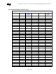
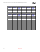
1x Timing Domain 2x/4x Timing Domain Miscellaneous Signals
AGPCLK
PIPE#
RBF#
WBF#
ST[2:0]
G_FRAME#
G_IRDY#
G_TRDY#
G_STOP#
G_DEVSEL#
G_REQ#
G_GNT#
G_PAR
SET #1
G_AD[15:0]
G_CBE[1:0]#
AD_STB0
AD_STB0#
SET #2
G_AD[31:16]
G_CBE[3:2]#
AD_STB1
AD_STB1#
SET #3
SBA[7:0]
SB_STB
SB_STB#
USB+
USB-
OVRCNT#
PME#
TYPDET#
PERR#
SERR#
INTA#
INTB#