
Mobile Intel Pentium 4 Processor - M and Intel 845MP/MZ Chipset Platform Design Guide

Mobile Intel
®
Pentium
®
4 Processor-M and Intel
®
845MP/845MZ Chipset Platform
Design Guide 9
R
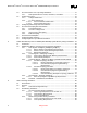
Figures
Figure 1. Typical System Block Diagram ................................................................................. 20
Figure 2. Cross-Sectional View of 2:1 Ratio ............................................................................ 27
Figure 3. GTLREF Routing ...................................................................................................... 28
Figure 4. Processor Topology .................................................................................................. 30
Figure 5. SS Topology for Address and Data .......................................................................... 31
Figure 6. CC Topology With ODT ............................................................................................ 33
Figure 7. CC Topology Without ODT ....................................................................................... 33
Figure 8. THRMTRIP# Circuit Recommendation..................................................................... 35
Figure 9. Routing Illustration for FERR#, IERR#, PROCHOT#, and THRMTRIP#.................. 36
Figure 10. Routing Illustration for LINT1/INTR, LINT0/NMI, DPSLP#, SLP#, STPCLK#,
IGNNE#, SMI# and A20M#, CPUPERF#, and PWRGOOD- Topology 2, 2A .......... 37
Figure 11. Routing Illustration INIT# ........................................................................................ 37
Figure 12. Voltage Translator Circuit of Topology#1 and #2B ................................................. 38
Figure 13. Voltage Regulator Block Diagram........................................................................... 41
Figure 14. Typical VCCIOPLL, VCCA, and VSSA Power Distribution ..................................... 42
Figure 15. Filter Recommendation........................................................................................... 43
Figure 16. Example Component Placement for PLL Filter....................................................... 44
Figure 17. Power On Sequencing Diagram ............................................................................. 45
Figure 18. Power Off Sequencing Diagram ............................................................................. 45
Figure 19. Processor High Frequency Decoupling Placement Example ................................. 47
Figure 20. Data Signal Routing Topology ................................................................................ 56
Figure 21. DQ/CB to DQS Trace Length Matching Requirements .......................................... 58
Figure 22. SDQS to SCK/SCK# Trace Length Matching Requirements.................................. 60
Figure 23. Data Signal Group Routing Example ...................................................................... 61
Figure 24. SO-DIMM0, 1 Control Signal Routing Topology ..................................................... 62
Figure 25. Referencing Plane Stack-up ................................................................................... 63
Figure 26. Control Signal to SCK/SCK# Trace Length Matching Requirements ..................... 65
Figure 27. Control Routing Example ........................................................................................ 66
Figure 28. Command Signal Routing Topology 1 .................................................................... 67
Figure 29. Referencing Plane Stack-up ................................................................................... 69
Figure 30. Command Signal to SCK/SCK# Trace Length Matching Requirements ................ 70
Figure 31. Command Routing Example for Topology 1........................................................... 71
Figure 32. Command Signal Routing Topology ....................................................................... 72
Figure 33. Referencing Plane Stack-up ................................................................................... 73
Figure 34. Command Signal to SCK/SCK# Trace Length Matching Requirements ................ 75
Figure 35. Command Routing Example for Topology 2........................................................... 76
Figure 36. DDR Clock Routing Topology (SCK/SCK#[2:0])..................................................... 77
Figure 37. Ground Referencing Plane Stack-up ...................................................................... 78
Figure 38. SCK to SCK# Trace Length Matching Requirements............................................. 80
Figure 39. Clock Pair Trace Length Matching Requirements .................................................. 81
Figure 40. DDR Feedback (RCVEN#) Routing Topology ........................................................ 82
Figure 41. AGP Layout Guidelines........................................................................................... 89
Figure 42. Intel 845MP/845MZ PLL0 Filter .............................................................................. 95
Figure 43. Intel 845MP/845MZ PLL1 Filter .............................................................................. 96
Figure 44. Hub Interface Routing Example.............................................................................. 97
Figure 45. Single HUBREF Voltage Divider ............................................................................. 99
Figure 46. Locally Generated HUBREF Divider ....................................................................... 99
Figure 47. Connection Requirements for Primary IDE Connector ......................................... 102
Figure 48. Connection Requirements for Secondary IDE Connector .................................... 103
Figure 49. PCI Bus Layout Example ...................................................................................... 104
Figure 50. ICH3-M AC’97 – Codec Connection ..................................................................... 105