
Mobile Intel Pentium 4 Processor - M and Intel 845MP/MZ Chipset Platform Design Guide


Mobile Intel
®
Pentium
®
4 Processor-M and Intel
®
845MP/845MZ Chipset Platform
Design Guide 97
R
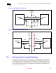
8. Hub Interface
The MCH-M and ICH3-M ballout assignments have been optimized to simplify the Hub Interface
routing between these devices. Intel recommends that the Hub Interface signals be routed directly from
the MCH-M to ICH3-M with all signals referenced to VSS. Layer transition should be kept to a
minimum. If a layer change is required, use only two vias per net and keep all data signals and associated
strobe signals on the same layer. The Hub Interface signals are broken into two groups: data signals (HL)
and strobe signals (HL_STB).
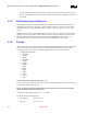
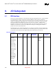
Figure 44. Hub Interface Routing Example
ICH3-M MCH-M
CLK
Synthesizer
CLK66 CLK66
HI[11:0]
HI_STB
HI_STB#
8.1. Hub Interface Routing Guidelines
This section documents the routing guidelines for the 10-bit hub interface. This hub interface connects
the ICH3-M and the MCH-M. The hub interface uses a compensation signal to adjust buffer
characteristics to the specific board characteristic. The hub interface requires Resistive Compensation
(RCOMP).
The trace impedance must equal 55
Ω ± 15%.
Table 35. Hub Interface RCOMP Resistor Values
Component Trace Impedance HICOMP Resistor Value HICOMP Resistor Tied to
ICH3-M 55 ohms ±15% 36.5 Ω ± 1% VSS
MCH-M 55 ohms ± 15% 36.5 Ω ± 1% Vcc1_8
8.2. Hub Interface Data Signals
These data signal traces should be routed 4 mils wide with 8 mils trace spacing (4 on8) and 12 mils
spacing from other signals. In order to break out of the MCH-M and ICH3-M packages, the hub interface
data signals can be routed 5-mils wide 5-mils spacing. The signal must be separated to 5-mils width with
10-mils spacing within 300 mils from the package.