
Mobile Intel Pentium 4 Processor - M and Intel 845MP/MZ Chipset Platform Design Guide


Mobile Intel
®
Pentium
®
4 Processor-M and Intel
®
845MP/845MZ Chipset Platform
98 Design Guide
R
The maximum hub interface data signal trace length is six inches. Each data signal must be matched
within
± 200 mils of the HL_STB differential pair. There is no explicit matching requirement between
the individual data signals.
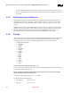
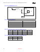
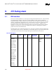
Table 36. Hub Interface Signals
Signal Max
length
(inch)
Width
(mils)
Space
(mils)
Mismatch
length
(mils)
Relative To Space with
other signals
(mils)
Notes
HUB_PD[10:0] 6 4 8 ±200 Differential
HUB_PSTRB
pair
12
HUB_PSTRB
and
HUB_PSTRB#
6 4 8 ±200 Data lines 12 HUB_PSTR
B and
HUB_PSTR
B# must be
the same
length (±10
mils)
8.3. Hub Interface Strobe Signals
The hub interface strobe signals should be routed as a differential pair, 4-mils wide with 8-mils trace
spacing (4 on 8) and 12-mils spacing from other signals. This strobe pair should have a minimum of 12
mils spacing from any adjacent signals. The maximum length for the strobe signals is six inches. Each
strobe signal must be the same length, and each data signal must be matched to within
± 200 mils of the
strobe signals.
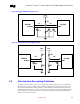
8.4. HUBREF Generation/Distribution
HUBREF is the hub interface reference voltage. Depending on the buffer mode, the HUBREF voltage
requirement must be set appropriately for proper operation. See the table below for the HUBREF voltage
specifications and the associated resistor recommendations for the voltage divider circuit.
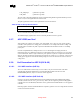
Table 37. Hub Interface HUBREF Generation Circuit Specifications
HUBREF Voltage Specification
(V)
Recommended Resistor Values for the HUBREF Divider
Circuit (Ohm)
½ VCC1_8 ± 4% R1 = R2 = 301 ± 1%
The single HUBREF divider should not be located more than four inches away from either the MCH-M
or ICH3-M. If the single HUBREF divider is located more than four inches away, locally generated hub
interface reference dividers should be used instead. The reference voltage generated by a single
HUBREF divider should be bypassed to ground with a 0.1-µF capacitor (C1) and at each component
with a 0.01-µF capacitor (C2) located close to the component HUBREF pin Figure 45. If the reference
voltage is generated locally, the bypass capacitor (0.01 µF) needs to be close to the component HUBREF
pin Figure 46.