
Voltage Regulator-Down (VRD) 10.0 Design Guide Addendum

R
VRD Design Guide Addendum
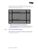
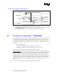
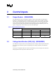
Figure 2: VRD Phase Orientation
PHASES
SOCKET SOCKET
North
South
East
West
Layout with north
phase placement
Layout with east
phase placement
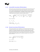
PHASES
CAVITY
CAVITY
Reference
Node
Reference
Node
PHASES
SOCKET SOCKET
North
South
East
West
Layout with north
phase placement
Layout with east
phase placement
PHASES
CAVITY
CAVITY
Reference
Node
Reference
Node
2.3 TOB: Voltage Tolerance Band (REQUIRED)
Processor load line specifications must be guaranteed across component process variation, system
temperature extremes, and age degradation limits. For the Pentium 4 processor Extreme Edition
supporting Hyper-Threading Technology, the VRD topology and component selection must
maintain a 3-sigma tolerance of +/-19mV around the typical load line (see Table 2). The critical
parameters include voltage ripple, VRD controller tolerance, and current sense tolerance.
Individual tolerance components will vary among designs; the processor requires only that the
total error stack-up stay within the defined +/-19mV at the FMB limits.
2.3.1 Sources of Voltage Deviation & Input Parameters
The standard VRD tolerance band (TOB) can be sliced into three main categories: controller
tolerance, current sense variation, and voltage ripple.
Controller tolerance is determined by the DAC accuracy (digital to analog conversion) and DC
offset of the internal controller circuitry (i.e. op amp offset). These tolerance parameters are
functions of the operating voltage associated with the programmed VID (defined in Table 1).
Internal controller circuitry also includes a tolerance associated with current sense signal
conversion that must be included in the TOB calculation. Consult the controller data sheet or
vendor for the particular component specifications.
VRD current sensing occurs by processing a sensed voltage across a component in the direct
output current path. Current conversion occurs with knowledge of the device resistance. The
tolerance of this sense method is directly aligned with the sense element’s tolerance. For
inductor, resistor, and FET sensing, the series resistance tolerance of the sense component is a
critical factor for calculating the TOB. Integrating capacitors are part of the inductor current
sense circuit and the manufacturing tolerance including thermal drift must be identified to ensure
correct TOB calculations. For inductor and FET sensing, thermal compensation (see section 2.4)
is required to maintain a linear load line across the full, operational system temperature range.