
Voltage Regulator-Down (VRD) 10.0 Design Guide Addendum

R
VRD Design Guide Addendum
Peak ripple must not exceed +/-5mV at the VRD measurement nodes. Ripple is typically
suppressed by increasing the value of the output inductance or by increasing the value/quantity of
ceramic capacitors in the high frequency filter (see 2.9).
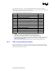
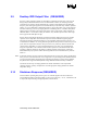
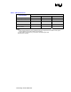
Table 3: Input parameters for VRD TOB calculation
Parameter Definition Units
I
dyn
FMB defined current step amplitude
1
A
I
max
Maximum FMB load current
1
A
k
C
Tolerance of CS capacitance
2 3
[±% @ 3-σ]
k
ESR
Tolerance of inductor ESR
4 6
[±% @ 3-σ]
k
gm
Controller tolerance of current signal conversion [±% @ 3-σ]
k
L
Tolerance of output inductance
4
[±% @ 3-σ]
k
RDS
Tolerance of FET RDS-ON
4
[±% @ 3-σ]
k
rsense
Tolerance of sense resistor
4
[±% @ 3-σ]
k
VID
Controller reference voltage (VID) tolerance [±% @ 3-σ]
n
ph
Number of independent phases in VRD -
n
rsense
Number of sense resistors -
R
AVP
AVP (Socket Load Line) resistance
[Ω]
V
ripple
Peak ripple voltage: Max = 5mV peak [±V]
V
TC
Thermal compensation transient error [±V]
NOTES:
1: See Table 1
2: Statistical root-sum-square may be applied if more than one component is used
3: Tolerance is to include parameter thermal drift across operational temperature
4: Thermal variation of parameter is included in VTC if thermal compensation is applied
5: All parameter tolerances are defined at 3-sigma. Many vendors define some common parameters, such as
inductor tolerance and inductor ESR, at 6-sigma. These numbers should be translated to 3-sigma to
obtain an accurate TOB calculation.
6: Vendors commonly refer to this parameter as RDC and it is generally a 6-sigma tolerance value
2.3.2 TOB: Tolerance Band Calculation
Reference TOB equations for each major current sense topology are provided in the next three
subsections. Equations are presented in a manner for simple entry into a spreadsheet to simplify
TOB calculation and design iterations.