
Voltage Regulator-Down (VRD) 10.0 Design Guide Addendum

R
VRD Design Guide Addendum
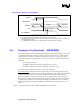
2.9 Desktop VRD Output Filter (REQUIRED)
Processor voltage regulators include an output filter to minimize transient noise on the Vcc rail.
Design analysis determined that the most cost efficient filter solution, for satisfying load line
requirements, incorporates 680 µF aluminum-poly capacitors with 5mOhm average ESR. High
frequency noise and ripple suppression is best minimized by 22 µF multi-layer ceramic capacitors
(MLCC’s). It is recommended to maximize the MLCC count in the socket cavity to help suppress
transients induced by processor packaging hardware. Remaining MLCC’s should be first placed
adjacent to the socket edge in the region between the socket cavity and the voltage regulator. If
additional MLCC’s are needed to satisfy the load line, they should be placed on the socket edge
that is opposite the VRD adjacent edge.
Prescott Processor Dynamic VID mode of operation is directly impacted by the choice of bulk
capacitors in the output filter. If the Pentium 4 processor Extreme Edition supporting Hyper-
Threading Technology motherboard design is to be compatible with the Prescott processor, it is
recommended to minimize Vcc setting time during Dynamic VID operation to hasten the speed of
power and core temperature reduction. The speed of recovery is directly related to the RC time
constant of the output filter. To ensure adequate thermal recovery time, it is recommended to
design the output filter with a minimal amount of bulk capacitance with minimum ESR, while
providing a sufficient amount of decoupling to maintain load line requirements. At this time,
680uF aluminum poly capacitors with 5 mΩ average ESR have been identified as the preferred
solution. =
Note: A load line selection circuit is required to switch between the two processor voltage specifications
if the processor code named Prescott is to be supported in a system designed for Intel® Pentium®
processor Extreme Edition supporting Hyper-Threading Technology in socket 478. In addition,
the platform must support the full Dynamic Voltage Identification functionality of VRD10.0.
Consult the relevant chip-set design guidelines for further information on the output filter
capacitor selection, quantity, and placement. Consult appropriate design guidelines for mobile
output filter design.
2.10 Shutdown Response (REQUIRED)
Once the VRD is operating after power up, if it sees a disable signal in the form of either de-
asserted Output Enable or VID [4:0] (VID5 is a don’t care in this case) = 11111, it should turn off
its output (the output should go to high impedance) within 500 ms.