
Voltage Regulator-Down (VRD) 10.0 Design Guide Addendum

R
VRD Design Guide Addendum
3 Control Inputs
3.1 Output Enable (REQUIRED)
The VRD should accept an input signal to enable the output. When disabled, the VRD output
should be in a high-impedance state and should not source current. Once the VRD is operating
after power-up, it should respond to a de-asserted Output Enable by turning off its output within
500 ms. When Output Enable is pulled low during the shutdown process, the VRD should not
exceed its previous voltage level regardless of the VID setting during the shutdown process. No
negative voltage below –100 mV may be present at the VRD output.
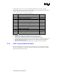
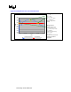
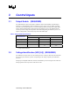
Table 4. Output Enable Specifications
Specification
Design Parameter
Minimum Maximum Units
Pull-Up Voltage Range 0 V
CC
VID
Pull-Up Resistor1 1 k 2.6 k Ohms
V
IH
0.8 Volts
V
IL
0.3 Volts
NOTES:
1. Range includes tolerances
3.2 Voltage Identification (VID [5:0]) (REQUIRED)
The VRD must accept six lines to set the nominal processor voltage as defined by the table below.
Six processor pins will have a pattern corresponding to the voltage required by the individual
processor.
VID [4:0] are compatible with Intel
®
Xeon™ and Pentium 4 processors using five-bit VID codes.
VID [5:0] will be used on processors with six-bit codes.