
Voltage Regulator-Down (VRD) 10.0 Design Guide Addendum


R
VRD Design Guide Addendum
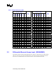
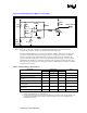
Table 6. Voltage Identification (VID)
Processor Pins
(0 = low, 1 = high)
Processor Pins
(0 = low, 1 = high)
VID5
VID4
VID3
VID2
VID1
VID0
Vout
(V)
VID5
VID4
VID3
VID2
VID1
VID0
Vout
(V)
0 0 1 0 1 0 0.8375 0 1 1 0 1 0 1.2125
1 0 1 0 0 1 0.8500 1 1 1 0 0 1 1.2250
0 0 1 0 0 1 0.8625 0 1 1 0 0 1 1.2375
1 0 1 0 0 0 0.8750 1 1 1 0 0 0 1.2500
0 0 1 0 0 0 0.8875 0 1 1 0 0 0 1.2625
1 0 0 1 1 1 0.9000 1 1 0 1 1 1 1.2750
0 0 0 1 1 1 0.9125 0 1 0 1 1 1 1.2875
1 0 0 1 1 0 0.9250 1 1 0 1 1 0 1.3000
0 0 0 1 1 0 0.9375 0 1 0 1 1 0 1.3125
1 0 0 1 0 1 0.9500 1 1 0 1 0 1 1.3250
0 0 0 1 0 1 0.9625 0 1 0 1 0 1 1.3375
1 0 0 1 0 0 0.9750 1 1 0 1 0 0 1.3500
0 0 0 1 0 0 0.9875 0 1 0 1 0 0 1.3625
1 0 0 0 1 1 1.0000 1 1 0 0 1 1 1.3750
0 0 0 0 1 1 1.0125 0 1 0 0 1 1 1.3875
1 0 0 0 1 0 1.0250 1 1 0 0 1 0 1.4000
0 0 0 0 1 0 1.0375 0 1 0 0 1 0 1.4125
1 0 0 0 0 1 1.0500 1 1 0 0 0 1 1.4250
0 0 0 0 0 1 1.0625 0 1 0 0 0 1 1.4375
1 0 0 0 0 0 1.0750 1 1 0 0 0 0 1.4500
0 0 0 0 0 0 1.0875 0 1 0 0 0 0 1.4625
1 1 1 1 1 1 OFF
1
1 0 1 1 1 1 1.4750
0 1 1 1 1 1 OFF
1
0 0 1 1 1 1 1.4875
1 1 1 1 1 0 1.1000 1 0 1 1 1 0 1.5000
0 1 1 1 1 0 1.1125 0 0 1 1 1 0 1.5125
1 1 1 1 0 1 1.1250 1 0 1 1 0 1 1.5250
0 1 1 1 0 1 1.1375 0 0 1 1 0 1 1.5375
1 1 1 1 0 0 1.1500 1 0 1 1 0 0 1.5500
0 1 1 1 0 0 1.1625 0 0 1 1 0 0 1.5625
1 1 1 0 1 1 1.1750 1 0 1 0 1 1 1.5750
0 1 1 0 1 1 1.1875 0 0 1 0 1 1 1.5875
1 1 1 0 1 0 1.2000 1 0 1 0 1 0 1.6000
NOTES:
1. Output disabled – the same as de-asserting the output enable input (Section 3.1).
3.3 Differential Remote Sense Input (REQUIRED)
The PWM controller should include differential sense inputs to compensate for an output voltage
offset of ≤ 300 mV in the power distribution path. The remote sense lines should draw no more
than 10 mA, to minimize offset errors. Refer to Section 2.2 for measurement location.