
Voltage Regulator-Down (VRD) 10.0

Processor Voltage Requirements
R
20 VRD Design Guide
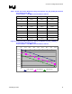
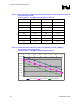
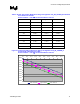
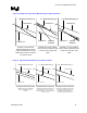
2.3 TOB: Voltage Tolerance Band (REQUIRED)
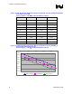
Processor loadline specifications must be guaranteed across component process variation, system
temperature extremes, and age degradation limits. The VRD topology and component selection
must maintain a 3-sigma tolerance of The VRD Tolerance Band around the typical loadline (see
Section 2.2). The critical parameters include voltage ripple, VRD controller tolerance, and current
sense tolerance. Individual tolerance components will vary among designs; the processor requires
only that the total error stack-up stay within the defined VR configuration tolerance band under the
conditions defined in Table 4.
2.3.1 Sources of Voltage Deviation and Input Parameters
The standard VRD tolerance band (TOB) can be sliced into three main categories: controller
tolerance, current sense variation, and voltage ripple.
Controller tolerance is determined by the DAC accuracy (digital to analog conversion) and DC
offset of the internal controller circuitry (i.e., op amp offset). These tolerance parameters are
functions of the operating voltage associated with the programmed VID (defined in Table 4).
Internal controller circuitry also includes a tolerance associated with current sense signal
conversion that must be included in the TOB calculation. Consult the controller data sheet or
vendor for the particular component specifications.
VRD current sensing occurs by processing a sensed voltage across a component in the direct
output current path. Current conversion occurs with knowledge of the device resistance and/or
impedance. The tolerance of this sense method is directly aligned with the sense element’s
tolerance. For inductor, resistor, and FET sensing, the series resistance tolerance of the sense
component is a critical factor for calculating the TOB. Integrating capacitors are part of the
inductor current sense circuit and the manufacturing tolerance including thermal drift must be
identified to ensure correct TOB calculations. For inductor and FET sensing, thermal
compensation (see Section 2.4) is required to maintain a linear loadline across the full, operational
system temperature range.
Peak ripple should not exceed ± 5 mV at the VRD measurement nodes. Ripple is typically
suppressed by increasing the value of the output inductance or by increasing the value/quantity of
ceramic capacitors in the high frequency filter (see Section 2.10).