
Voltage Regulator-Down (VRD) 10.0

Processor Voltage Requirements
R
VRD Design Guide
21
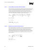
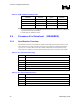
Table 11. Input Parameters for VRD TOB Calculation
Parameter Definition Units
I
dyn
Defined current step amplitude
1
A
I
max
Maximum load current
1
A
k
C
Tolerance of CS capacitance
2 3
[±% @ 3-σ]
k
ESR
Tolerance of inductor ESR
4 6
[±% @ 3-σ]
k
gm
Controller tolerance of current signal conversion [±% @ 3-σ]
k
L
Tolerance of output inductance
4
[±% @ 3-σ]
k
RDS
Tolerance of FET RDS-ON
4
[±% @ 3-σ]
k
rsense
Tolerance of sense resistor
4
[±% @ 3-σ]
k
VID
Controller reference voltage (VID) tolerance [±% @ 3-σ]
n
ph
Number of independent phases in VRD -
n
rsense
Number of sense resistors -
R
AVP
AVP (Socket Loadline) resistance
[
Ω]
V
ripple
Peak ripple voltage: Max = 5 mV peak [±V]
V
TC
Thermal compensation transient error [±V]
NOTES:
1. See Table 4
2. Statistical root-sum-square may be applied if more than one component is used
3. Tolerance is to include parameter thermal drift across operational temperature
4. Thermal variation of parameter is included in VTC if thermal compensation is applied
5. All parameter tolerances are defined at 3-sigma. Many vendors define some common parameters, such
as inductor tolerance and inductor ESR, at 6-sigma. These numbers should be translated to 3-sigma to
obtain an accurate TOB calculation.
6. Vendors commonly refer to this parameter as RDC and it is generally a 6-sigma tolerance value. Quite
often RDC is not, or is loosely, specified and engineering evaluation of the specific inductor
manufacturing variables is needed to determine a reasonable RDC variation.
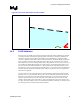
2.3.2 TOB: Tolerance Band Calculation
Reference TOB equations for each major current sense topology are provided in the next three
subsections. Equations are presented in a manner for simple entry into a spreadsheet to simplify
TOB calculation and design iterations. Contact your chosen PWM controller vendor for exact
formulas.