
Voltage Regulator-Down (VRD) 10.0

Processor Voltage Requirements
R
24 VRD Design Guide
2.5 Processor Electrical and Thermal Current Support
(EXPECTED)
System boards supporting Intel
processors in Socket 478 must have voltage regulator designs
compliant to applicable processor’s electrical and electrical-thermal standards. This includes full
electrical support of Iccmax specifications and robust cooling solutions to support the VRD
thermal design current (VR TDC) indefinitely within the envelope of system operating conditions
(see Table 4).
Processor VR TDC is the sustained (DC equivalent) current parameter that is to be used for
voltage regulator thermal design with supporting Thermal Monitor circuitry (see Section 6.2). At
TDC, switching FETs reach maximum temperature heating the motherboard layers, processor
socket, and neighboring components to the pass/fail boundary of thermal limits. Actual component
and board temperatures are established by the envelope of the system’s operating conditions and
component physical properties. This includes voltage regulator layout, processor fan selection,
ambient temperature, chassis configuration, component selection, etc.
In some instances the processor’s VRD will also power other motherboard components such as the
chipset. Under these conditions, the VRD may supply current above the stated Iccmax and/or TDC
limits; VR designers must budget this additional current support in final VRD designs while
remaining compliant to electrical and thermal specifications.
2.6 Stability (EXPECTED)
The VRD must be unconditionally stable under all specified output voltage ranges and current
transients. The VRD should operate in a no-load condition: i.e., with no processor installed.
Normally the no-processor VID code will be x1111, disabling the VRD (Section 2.11).
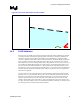
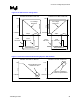
2.7 Processor Power Sequencing (REQUIRED)
The VRD must correctly sequence power in accordance with Intel processor requirements. Figure
7 is a block diagram of the VRD connectivity with necessary signals and relevant power rails.
Figure 8 provides the timing protocol for these signals and power rails in socket 478 platforms.