
Voltage Regulator-Down (VRD) 10.0

Processor Voltage Requirements
R
VRD Design Guide
25
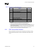
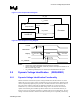
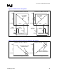
Figure 7. Power Sequence Block Diagram
V
CC
VR
Output Enable
V
CC
VID VR
Processor
V
CC
VID
VID_PWRGD
V
CC
V
CC
_
PWRGD
VID_[5.0]
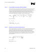
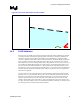
Figure 8. Power Sequence Timing Diagram
Vcc_PWRGD
Vcc
VID Invalid VID Valid
VIDPWRGD
VID[5:0]
1ms min
10 ms max
VID Invalid
0 ms min
10 ms max
VccVID
NOTES:
• VccVID comes up at the application of system power to the VccVID VR.
• VccVID VR generates VID_PWRGD, to latch the processor’s VID outputs and enable Vcc VR
after the VccVID supply is valid.
• Vcc_PWRGD is generated by the Vcc VR and may be used elsewhere in the system.
2.8 Dynamic Voltage Identification (REQUIRED)
2.8.1 Dynamic-Voltage Identification Functionality
VRD10 architecture includes the Dynamic Voltage Identification (D-VID) feature set, which
enables the processor to reduce power consumption and processor temperature. Reference VID
codes are dynamically updated by the processor to the VRD controller via the VID bus when a
low power state is initiated. VID codes are updated sequentially in 12.5 mV steps and are
transmitted every 5 microseconds until the final voltage code is encountered. Processors are
capable of transitioning from standard operational VID levels to the minimum table entry of
0.8375V. They are also capable of returning to a higher VID code in a similar manner. The low
voltage code will be held for a minimum of 50 microseconds prior to sequentially transitioning