
Voltage Regulator-Down (VRD) 10.0

Processor Voltage Requirements
R
VRD Design Guide
27
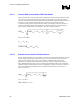
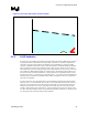
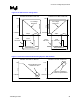
Figure 9. Processor D-VID Loadline Transition States
2.8.2 D-VID Validation
Intel processors are capable of generating numerous D-VID states and the VRD must be designed
to properly transition to and function at each possible code. However, exhaustive validation of
each state is unnecessary and impractical. Validation can be simplified by verifying the VRD
conforms to loadline requirements, tolerance band specifications, and D-VID timing requirements.
Then, by default, each processor D-VID state will be valid. The key variables for Vcc under D-
VID conditions are processor loading, starting VID, ending VID, and Vcc slew rate. The Vcc slew
rate is defined by VRD bulk decoupling, the output inductors, the switching FET resistance, and
the processor load. This indicates that the Vcc slewing will have an exponential behavior, where
the response to code ‘n+1’ takes longer to settle than code ‘n’. As a result, a test from maximum to
minimum and from minimum to maximum will be sufficient to guarantee slew rate requirements
and VID code regulation.
To ensure support for any valid VID reference, testing should be performed from the maximum
table entry of 1.6 V to the minimum value of 0.8375 V. The VRD must ensure that this 0.7625 V
transition occurs within 50 microseconds of the final VID code, in 350 microseconds. Slew rate
timing is referenced from 0.4 V on the rising edge of the initial VID code to the time the final
voltage is settled within 5 mV of the final Vcc value. Intel testing has noted a 10% change to the
Vcc slew rate between VRD no load (5 A) and full load (VR TDC) conditions. For this reason, the
Vcc slewing must be tested under both loading conditions.