
Voltage Regulator-Down (VRD) 10.0

Processor Voltage Requirements
R
VRD Design Guide
31
Maximum overshoot in socket 478 is validated by monitoring the voltage across the recommended
test pins (defined in Section 2.2) while applying a current load release across the socket Vcc and
Vss pin field. Amperage values for performing this validation under each VRD design
configuration are identified in Table 15. The platform voltage regulator output filter must be
stuffed with a sufficient quality and number of capacitors to ensure that overshoot says above VID
for a time no longer than T
OS
-
MAX
and never exceeds the maximum amplitude of
VID+V
OS
_
MAX
.
Measurements are to be taken using an oscilloscope with a 20 MHz bandwidth.
Boards in violation must be redesigned for compliance to avoid processor damage.
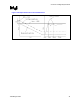
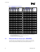
Table 15. Intel
®
Processor Current Release Values for Overshoot Testing
VR Configuration Starting Current Ending Current Dynamic Current Step
478_VR_CONFIG_A 75 A 5 A 70 A
478_VR_CONFIG_B 60 A 5 A 55 A
478_VR_CONFIG_C 55 A 5 A 50 A
478_VR_CONFIG_D 75 A 5 A 70 A
To prevent processor damage, VRD designs should comply to overshoot specifications across the
full loadline tolerance band window (see Section 2.2). When validating a system’s overshoot, a
single measurement is statistically insignificant and cannot represent the response variation seen
across the entire high volume manufacturing population of VRD designs. A typical design may fit
in the loadline window; however designs residing elsewhere in the tolerance band distribution may
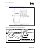
violate the Vcc overshoot specifications. Figure 13 provides an illustration of this concept. A
typical board will have the Vcc zero current voltage (Vzc) centered in the loadline window at
VID-TOB; for this example, assume TOB is 20 mV waveform A). Now assume that the VRD has
maximum overshoot amplitude of VOS_MAX = 50 mV above VID. Under this single case, the
overshoot aligns with the specification limit and there is zero margin to violation. Under
manufacturing variation Vzc can drift to align with VID (waveform B). This drift will shift the
overshoot waveform by the same voltage level. Since this example has zero overshoot amplitude
margin, this increase in Vzc due to manufacturing drift will yield a 20 mV overshoot violation
which will reduce the processor life span. To address this issue in validation, a voltage margining
technique can be employed to ensure overshoot amplitudes stay below a safe value. This technique
translates the specification baseline from VID to a VRD validation baseline of Vzc + VOS_MAX,
which defines a test limit for specification compliance across the full TOB range:
Equation 1: Overshoot Voltage Limit
V
OS
< Vzc + VOS_MAX
This equation is to be used during validation to ensure overshoot is in compliance to specifications
across high volume manufacturing variation. In addition, the overshoot duration must be reference
to Vzc and cannot exceed this level by more than 25 µs.