
Voltage Regulator-Down (VRD) 10.0

Control Inputs
R
VRD Design Guide
37
3 Control Inputs
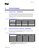
3.1 Output Enable (REQUIRED)
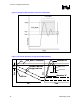
The VRD controller is to recognize the Output Enable signal to assert/disable Vcc regulation.
When disabled, the VRD output is to function in a high-impedance state and not source current.
Once the VRD is operating after power-up, it should respond to a de-asserted Output Enable by
turning off Vcc within 500 ms. When Output Enable is pulled low during the shutdown process,
the VRD should not exceed its previous voltage level regardless of the VID setting during the
shutdown process.
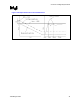
Table 16. Output Enable Specifications
Specification
Design Parameter
Minimum Maximum Units
Pull-Up Voltage Range 0 VCC VID Volts
Pull-Up Resistor1 1 k 2.6 k Ohms
V
IH
0.8 - Volts
V
IL
- 0.3 Volts
NOTES: 1. Range includes tolerances
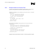
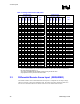
3.2 Voltage Identification (VID [5:0]) (REQUIRED)
The VRD is to read a five or six bit code transmitted by the processor across the VID bus to set
the reference Vcc value. A comprehensive list of all VID codes is provided in Table 18. VID
buffer signaling requirements are provided in Table 17.
Table 17. VID Signal Specifications
Specification
Design Parameter
Minimum Maximum Units
Pull-Up Voltage Range 3.135 3.465 Volts
Pull-Up Resistor
1
950 1050 Ohms
VIH
2
0.8 - Volts
VIL
2
- 0.4 Volts
VID Buffer leakage current 100 200 Microamperes
NOTES:
1. Range includes tolerances. Pull-up resistors should not be integrated into the PWM controller (values
may be adjusted on the system board for signal integrity).
2. Other platform components may use VID inputs and require tighter limits.
3. Table shown for reference.