
Voltage Regulator-Down (VRD) 10.0


Output Indicators
R
44 VRD Design Guide
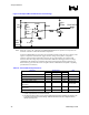
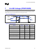
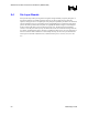
Figure 15: Example VRD Thermal Monitor Circuit Design
0.1uF
Q1
3904
LM393
Vcc(5)
Rtc
6.8k
THMSTR
7.5kΩ
+
-
R3
1kΩ
R2
499Ω
130Ω
R1
1kΩ
680Ω
Rpu
130Ω
Vcc(5)
Vtt
PROCHOT#
Note: Where R
2
= R
1
/R
3
* R
tc
. Thermister is NTHS0603N02N6801JR or equivalent. R
tc
represents the
thermister resistance at maximum allowable temperature.
Assertion of PROCHOT# is governed by the comparator (LM393) using the sensor voltage (at the
negative comparator terminal) and a trigger reference voltage (at the positive comparator
terminal). As the thermistor temperature increases due to system loading, the resistance will
decrease. When the voltage drop across the thermistor falls below the trigger reference voltage,
established by R1 and R2, the comparator will change state and bias the bipolar transistor (Q1).
When biased, Q1 provides the active low signal assertion of PROCHOT# compliant to signaling
specifications (see Table 20).
Table 20. Thermal Monitor Specifications
Specification Parameter
Min Typ Max
Units
V
TT
voltage - (V
TT
)
1
- Volts
V
CC
1
4.75 5.00 5.25 Volts
Transistor Q1 output ‘on’ (low) resistance - - 11 Ohms
PROCHOT# leakage current - - 200 Microamperes
Transition time20% to 80% signal rise for
PROCHOT#
0.550 100 -
Nanoseconds
Minimum time in or out of Thermal
Monitor state
1.0 - -
Milliseconds
RPU (Pull-up Resistor)
2
- 130 Ω ± 5% - Ohms
NOTES:
1. Consult Vtt specifications for min and max limits.
2. The thermal monitor circuit is to use a single motherboard pull up resistor to bias the Q1 collector. This
is provided in the PROCHOT# circuit design. Additional termination must not be integrated into the
thermal monitoring circuit.