
Voltage Regulator-Down (VRD) 10.0


Motherboard Power Plane Recommendations (EXPECTED)
R
50 VRD Design Guide
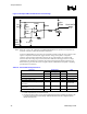
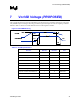
8.4 Six-Layer Boards
Six layer boards provide layout engineers with greater design flexibility. Adjacent plane pairs of
the same potential are not useful at higher frequencies, so the best approach is to maximize
adjacent, closely spaced Vcc/Vss plane pairs. The plane pair separated by the PCB core material is
of lesser importance since it is generally an order of magnitude larger in spacing than other plane
pairs in the stack-up. Because the Vss planes are typically full floods of copper, a well-designed
six-layer stack-up has four Vcc layers and two layers for Vss. The DC resistive requirements
(section 8.1) of the power delivery loop can still be met because the Vss floods are larger than the
Vcc floods, and the higher frequency needs are considered as there are four Vcc/Vss plane pairs to
deliver current and reduce inductance. In this example stack-up, the two Vss layers should be the
inner layers on each side of the PCB core, so that the stack-up is Vcc-Vss-Vcc-(core)-Vcc-Vss-
Vcc.