
Voltage Regulator-Down (VRD) 10.0

R
6 VRD Design Guide
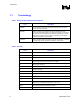
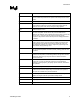
Revision History
Revision
Number
Description Revision Date
-001 • Initial Release. April 2003
-002 • Corrected load line formula in Section 2.2. November 2003
-003 • Added Section 1.1 Terminology and Table 2. Glossary.
• Section 2.2 added Tables 3 – 5, 10; modified Tables 6 – 9 and
Figures 1 –4.
• Added Section 2.3 TOB: Tolerance Band.
• Renumbered Sections 2.4 – 2.10 to Sections 2.5 – 2.11
• Added Section 2.8.1 Validation summary, Figures 10 – 11
• Added Section 2.9.1 Specification Overview and Figures 12 – 14.
• Added 2.9.2 Example: Socket Vcc Overshoot Test
• Modified Section 2.10
• Modified Section 4.2
• Modified Section 6.2
• Added Section 8 Motherboard Power Plane Recommendations
• Added Section 8.1 Minimize Power Path Resistance
• Added Section 8.2 Minimize Power Delivery Inductance
• Added Section 8.3 Four Layer Boards
• Added Section 8.4 Six Layer Boards
February 2004