
Voltage Regulator-Down (VRD) 10.0

Introduction
R
8 VRD Design Guide
1.1 Terminology
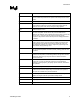
Table 1. Design Guideline Requirement Categories
Term Description
REQUIRED An essential feature of the design that must be supported to ensure correct
processor and VRD functionality.
EXPECTED A feature to ensure correct VRD and processor functionality that can be
supported using an alternate solution. The feature is necessary for consistency
among system and power designs and is traditionally modified only for custom
configurations. The feature may be modified or expanded by system OEMs if
the intended functionality is fully supported.
PROPOSED A feature that adds standard functionality to the VRD and, therefore, is included
as a design target. May be specified or expanded by system OEMs.
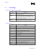
Table 2. Glossary
Term Description
Socket 478 Processor socket
DAC Digital to Analog Converter
DCR Direct Current Resistance
D-VID Dynamic Voltage Identification. A low power mode of operation where the
processor instructs the VRD to operate at a lower voltage.
ESL Effective series inductance
ESR Effective series resistance.
FET Field Effect Transistor
FMS Flexible Mobile Specifications for transportable platform design
FR 4 A type of printed circuit board (PCB) material
HVM High volume manufacturing
I
cc
, V
cc
Processor current, processor voltage
Loadline A mathematical model that describes voltage current relationship given system
impedance (R
LL
). The loadline equations is V
cc
= VID – I*R
LL
-
MOSFET Metal Oxide Semiconductor Field Effect Transistor
RDS-ON FET source to drain channel resistance when bias on.