
Voltage Regulator-Down (VRD) 10.1 Design Guide

Processor Vcc Requirements
R
14 Design Guide
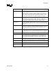
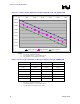
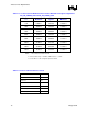
Table 2-2. Vcc Regulator Design Parameters
VR Configuration Iccmax
VR
TDC
Dynamic
Icc
R
LL
TOB
Maximum
VID
775_VR_CONFIG_04A 78 A 68 A 55 A 1.40 mΩ ±25 mV 1.4 V
775_VR_CONFIG_04B 119 A 101 A 95 A 1.00 mΩ ±19 mV 1.4 V
775_VR_CONFIG_05A 100A 85A 65A 1.00mΩ +/-19mV 1.4V
775_VR_CONFIG_05B 125A 115A 95A 1.00mΩ +/-19mV 1.4V
Refer to the relevant processor datasheet for mapping to the correct VR ConfigurationVRD
transient socket load line circuits should be designed to meet or exceed rated conditions defined in
Table 2-1. For example, 775_VR_CONFIG_04A requires a socket load line slope of 1.40 mΩ. A
transient socket load line slope of 1.0 mΩ will satisfy this requirement without adversely
impacting system performance or processor lifespan. This condition may be necessary when
supporting multiple processors with a single VRD design. However, the static load line condition
must be set to the recommended value unless explicitly stated otherwise in the processor
datasheet. Operating at a low load line resistance will result in higher processor operating
temperature, which may result in damage or a reduced processor life span. Processor temperature
rise from higher functional voltages may lead to operation at low power states which directly
reduces processor performance. Operating at a higher load line resistance will result in minimum
voltage violations which may result in system lock-up, “blue screening”, or data corruption.
Table 2-1 provides a comprehensive list of VRD10 LGA775 voltage regulator design
configurations. The configurations to be adopted by VRD hardware will depend on the specific
processors the design is intended to support. It is common for a motherboard to support
processors that require different VR configurations. In this case, the Vcc regulator design must
meet the specifications of all processors supported by that board. For example, If a motherboard is
targeted to support processors that require 775_VR_CONFIG_04A and 775_VR_CONFIG_04B,
then the voltage regulator must have the ability to support 101A of VR TDC, 119A of electrical
peak current, satisfy overshoot requirements of Section 2.7with a dynamic load step of 95 A,
satisfy a VRD tolerance band of ±19 mV (see Section 2.3), and have the ability to detect the
specific processor installed in the socket and automatically configure the load line slope (RLL) to
the correct value. VR configuration requirements will be defined in processor datasheets.
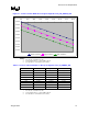
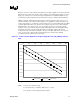
The following tables and figures show minimum and maximum voltage boundaries for each
socket load line design configuration defined in Table 2-1. V
CCTYP
socket load lines are provided
for design reference; designs should calibrate the socket load line to this case (centered in the load
line window, at the mean of the tolerance band). Different processors discussed in this design
guide can be shipped with different VID values. The reader should not assume that processors
with similar characteristics will have the save VID value. Typical values will range from 1.1 V to
1.6 V in 12.5 mV increments. A single load line chart and figure for each VRD design
configuration can represent functionality for each possible VID value. Tables and figures
presented as voltage deviation from VID provide the necessary information to identify voltage
requirements at any reference VID. This avoids the redundancy of publishing tables and figures
for each of the multiple cases.