
Voltage Regulator-Down (VRD) 10.1 Design Guide

Processor Vcc Requirements
R
Design Guide 15
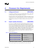
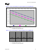
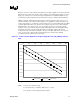
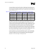
Figure 2-1. Socket Load Line Window for Design Configuration 775_VR_CONFIG_04A
-0.18 V
-0.16 V
-0.14 V
-0.12 V
-0.10 V
-0.08 V
-0.06 V
-0.04 V
-0.02 V
0.00 V
0 A 10 A 20 A 30 A 40 A 50 A 60 A 70 A 80 A
Vmax Load Line Vtyp Load Line Vmin Load Line
NOTES:
1. Presented as a deviation from VID.
2. Socket load line Slope = 1.4 mΩ, TOB = ±25 mV
3. Consult Table 2-1 for maximum current values
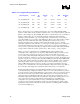
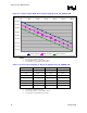
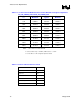
Table 2-3. Socket Load Line Window for Design Configuration 775_VR_CONFIG_04A
Icc Maximum Typical Minimum
0 A 0.000 V -0.025 V -0.050 V
10 A -0.014 V -0.039 V -0.064 V
20 A -0.028 V -0.053 V -0.078 V
30 A -0.042 V -0.067 V -0.092 V
40 A -0.056 V -0.081 V -0.106 V
50 A -0.070 V -0.095 V -0.120 V
60 A -0.084 V -0.109 V -0.134 V
70 A -0.098 V -0.123 V -0.148 V
80 A -0.112 V -0.137 V -0.162 V
NOTES:
1. Presented as a deviation from VID.
2. Socket load line Slope = 1.4 mΩ, TOB = ±25 mV
3. Consult Table 2-1 for maximum current values