
Voltage Regulator-Down (VRD) 10.1 Design Guide

Processor Vcc Requirements
R
Design Guide 17
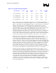
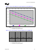
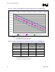
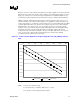
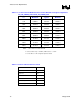
Reference nodes for socket load line measurements and voltage regulation are located in the land
field between the socket cavity and the voltage regulator region with the highest phase count (see
Figure 2-3); references for north and east phase configurations are identified in Table 2-5. It is
recommended to place motherboard test points at these locations to enable load line calibration.
VRD layout studies indicate that the highest phase count is best located north of the processor
with the controller to the southeast. This orientation is not suitable for routing sense lines to the
location discussed above, so Intel has provided dedicated processor lands which jumper the VRD
controller differential remote sense traces from a southeast connection to the center north land
field. These lines are routed across the processor package and dropped down to the optimal
regulation nodes of the motherboard power planes. The package traces are electrically isolated
from all die and package electrical networks, simply providing the voltage at the desired
motherboard sense node. In this configuration, the processor differential remote sense lands are
also to be used as the socket load line measurement reference and all socket electrical
specifications must be satisfied across these lands.
Figure 2-3. Socket Load Line Window for Design Configuration 775_VR_CONFIG_05A and
05B
-0.18 V
-0.16 V
-0.14 V
-0.12 V
-0.10 V
-0.08 V
-0.06 V
-0.04 V
-0.02 V
0.00 V
0 A 20 A 40 A 60 A 80 A 100 A 120 A 140 A
Vmax Load Line Vtyp Load Line Vmin Load Line
NOTE: 1: Presented as a deviation from VID
2: Socket load line Slope = 1.0mOhms, TOB Tolerance = +/-19mV
3: Consult Table 1 for VR configuration parameter details