
Voltage Regulator-Down (VRD) 10.1 Design Guide

Processor Vcc Requirements
R
20 Design Guide
To properly calibrate the socket load line parameter, the VR designer must excite the processor
socket with a current step that generates a voltage droop which must be checked against the load
line window requirements. Table 2-8 identifies the steady state and transient current values to use
for this calibration. For additional information, please consult the Socket Load Line Calculator for
the appropriate Intel processor.
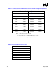
Table 2-6: Intel
®
Processor Current Step Values for Transient Socket Load Line Testing
VR Configuration Starting Current Ending Current Dynamic Current Step
775_VR_CONFIG_04A 23 A 78 A 55 A
775_VR_CONFIG_04B 24 A 119 A 95 A
775_VR_CONFIG_05A 35A 100A 65A
775_VR_CONFIG_05B 30A 125A 95A
VRD designs must be socket load line compliant across the full tolerance band window to avoid
data corruption, system lock-up, and reduced performance. When validating a system’s socket
load line, a single measurement is statistically insignificant and cannot represent the response
variation seen across the entire high volume manufacturing population of VRD designs. A typical
socket load line may fit in the specification window; however designs residing elsewhere in the
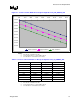
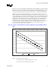
tolerance band distribution may violate the specifications. For example, Figure 2-4. Example A
shows a load line that is contained in the specification window and, in this single instance,
complies with Vccmin and Vccmax specifications. The positioning of this socket load line will
shift up and down as the tolerance drifts from typical to the design limits. Figure 2-4, Example B
shows that Vccmax limits will be violated as the component tolerances shift the load line to the
upper tolerance band limits. Figure 2-4, Example C shows that the Vccmin limits will be violated
as the component tolerances shift the load line to the lower tolerance band limits.
To satisfy specifications across high volume manufacturing variation, a typical socket load line
must be centered in the load line window and have a slope equal to the value specified in Table
2-1. Figure 2-4, Example A shows a socket load line that meets this condition. Under full 3-σ
tolerance band variation, the load line slope will intercept the Vccmax load line (Figure 2-4 ,
Example B) or Vccmin load line (Figure 2-4, Example C) limits.