
Voltage Regulator-Down (VRD) 10.1 Design Guide
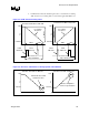

Processor Vcc Requirements
R
Design Guide 23
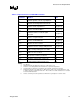
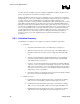
Table 2-7. Input Parameters for VRD TOB Calculation
Parameter Definition Units
I
dyn
Maximum dynamic current step amplitude
1
A
I
max
Maximum VR Configuration load current
1
A
k
C
Tolerance of CS capacitance
2 3
[±% @ 3-σ]
k
ESR
Tolerance of inductor DCR
4 6
[±% @ 3-σ]
k
gm
Controller tolerance of current signal
conversion
[±% @ 3-σ]
k
L
Tolerance of output inductance
4
[±% @ 3-σ]
k
RDS
Tolerance of FET RDS-ON
4
[±% @ 3-σ]
k
rsense
Tolerance of sense resistor
4
[±% @ 3-σ]
k
VID
Controller reference voltage (VID) tolerance
[±% @ 3-σ]
n
ph
Number of independent phases in VRD -
n
rsense
Number of sense resistors -
R
AVP
AVP (Socket Load Line) resistance
[Ω]
V
ripple
Peak ripple voltage: Max = 5mV peak [±V]
V
TC
Thermal compensation transient error [±V]
NOTES:
1. See Table 2-1.
2. Statistical RSS may be applied if more than one component is used.
3. Tolerance is to include parameter thermal drift across operational temperature.
4. Thermal variation of parameter is included in VTC if thermal compensation is applied.
5. All parameter tolerances are defined at 3-σ. Many vendors define some common parameters, such
as inductor tolerance and inductor DCR, at 6-σ. These numbers should be translated to 3-σ to obtain
an accurate TOB calculation.
6. Vendors commonly refer to this parameter as RDC and it is generally a 6-σ tolerance value.