
Voltage Regulator-Down (VRD) 10.1 Design Guide

Processor Vcc Requirements
R
26 Design Guide
2.5 Stability (EXPECTED)
The VRD must be unconditionally stable under all DC and transient conditions across the voltage
and current ranges defined in Table 2-2 through Table 2-4 and Figure 2-1 and Figure 2-2. The
VRD must also operate in a no-load condition: i.e., with no processor installed. Normally the no-
processor VID code will be 11111, disabling the VRD (see Table 9-1).
2.6 Dynamic Voltage Identification (REQUIRED)
2.6.1 Dynamic-Voltage Identification Functionality
VRD10 architecture includes the Dynamic Voltage Identification (D-VID) feature set, which
enables the processor to reduce power consumption and processor temperature. Reference VID
codes are dynamically updated by the processor to the VRD controller via the VID bus when a
low power state is initiated. VID codes are updated sequentially in 12.5 mV steps and are
transmitted every 5 microseconds until the final voltage code is encountered. Processors are
capable of transitioning from standard operational VID levels to the minimum table entry of
0.8375 V. They are also capable of returning to a higher VID code in a similar manner. The low
voltage code will be held for a minimum of 50 microseconds prior to sequentially transitioning
through the VID table to a new voltage reference which can be any higher VID code, but is
generally the original reference VID.
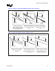
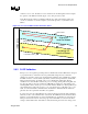
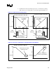
Figure 2-6 illustrates processor-operating states as the VID level is lowered. The diagram assumes
steady state, maximum current during the transition for ease of illustration. In this figure, the
processor begins in a high-load condition. Upon entering D-VID, the processor will shift to a low
power state and stop executing code (sequence 1 => 2). After reaching state 2, the processor
encounters a brief delay to prepare for low power operation then re-initiates code, resulting in
current draw and a load line IR drop to state 3. Sequencing from state 3 to 4 is a simplification of
the multiple steps from the original VID load line window to the low-voltage VID window.
Transition from state 4 to state 5 is an example of a load change during normal operation in the
low voltage VID setting. Transition from a low to high VID reference follows the reverse
sequence.
During a D-VID transition, Vcc must always reside above the minimum load line of the current
VID setting (see Figure 2-6). The load line values of each VID increment are required to match
the slope defined in Table 2-1. In addition, the voltage tolerance band and ripple specifications
defined in Table 2-1and Section 2.3 must be satisfied in this state. To expedite power reduction
and processor cooling, the VRD must lower the maximum Vcc value to reside within the low
voltage VID window within 50 microseconds of the final VID code transmission (see Figure 2-1
and Figure 2-7). The VRD must respond to a transition from low VID to high VID by regulating
the Vcc output to the range defined by the new VID code within 50 microseconds of the final
code transmission. Note: the minimum VID is not constant among all processors; the value will
vary with frequency and standard VID settings. This results in numerous possible D-VID states.
A simple and direct D-VID validation method is defined at the end of this section.
During a D-VID event, the processor load may not be capable of absorbing output capacitor
energy when the VID reference is lowered. As a result, reverse current may flow into the AC-DC
regulator’s input filter, potentially charging the input filter to a voltage above the over voltage
value. Upon detection of this condition, the AC-DC regulator will react by shutting down the AC-
DC regulator supply voltage. The VRD and AC-DC filter must be designed to ensure this