
Voltage Regulator-Down (VRD) 10.1 Design Guide

Processor Vcc Requirements
R
28 Design Guide
Vcc slew rate between VRD no load (5 A) and full load (VR TDC) conditions. For this reason,
the Vcc slewing must be tested under both loading conditions.
During the D-VID test defined in the previous paragraph, Vcc droop and undershoot amplitudes
must be limited to avoid processor damage and performance failures. If the processor experiences
a voltage undershoot due to D-VID transitions, an application initiated di/dt droop can
superimpose with this event and potentially violate minimum voltage specifications. Droop during
this D-VID test must be limited to 5 mV. This value was derived by calculating VRD tolerance
band improvements at the low D-VID current and voltage values. If the processor experiences an
overshoot due to D-VID transitions, an application initiated di/dt overshoot can superimpose with
this event and potentially violate overshoot specifications. Overshoot is permitted, but must be
properly budgeted with respect to the specifications defined in Section 2.7. Superposition of the
dynamic VID overshoot event and the overshoot resulting from the transient test defined in
Section 2.7, must not exceed the amplitude and time requirements defined in the overshoot
specification.
2.6.3 Validation Summary
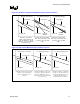
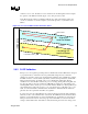
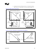
Consult Figure 2-7 and Figure 2-8 for graphic representation of validation requirements.
1. Constraints:
a. 762.5 mV ±5 mV transition must occur within 350 µs (see Figure 2-7)
b. Start time is referenced to 0.4 V on the rising edge of the initial D-VID code
c. End time is referenced to the steady state Vcc voltage after the final D-VID
code
d. Undershoot during maximum to minimum VID transition must be limited to
5 mV. This 5 mV is included within the ± 5 mV tolerance on the final VID
value defined under test condition a.
e. Overshoot observed when transitioning from minimum to maximum VID must
conform to overshoot specifications. Specifically, superposition of the dynamic
VID overshoot event and the overshoot resulting from the transient test defined
in Section 2.7 must not exceed the overshoot amplitude and time requirements
defined in the overshoot specification.
f. Care must be taken to avoid motherboard and component heat damage resulting
from extended operations with high current draw.
2. Validation exercises:
a. D-VID transition must be validated against above constraints from a starting
VID of 1.6 V to an ending VID of 0.8375 V with an applied 5 A Load.
b. D-VID transition must be validated against above constraints from a starting
VID of 1.6 V to an ending VID of 0.8375 V with an applied VR TDC Load.
c. D-VID transition must be validated against above constraints from a starting
VID of 0.8375 V to an ending VID of 1.6 V with an applied 5 A Load.