
Voltage Regulator-Down (VRD) 10.1 Design Guide

Processor Vcc Requirements
R
Design Guide 29
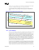
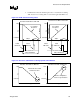
d. D-VID transition must be validated against above constraints from a starting
VID of 0.8375 V to an ending VID of 1.6 V with an applied VR TDC Load.
Figure 2-7. D-VID Transition Timing States
Vcc
Time (µs)
1.6V
1.6V
0.8375V
0.8375V
Initial
VID Code
Final
VID Code
Initial
VID Code
Final
VID Code
350µs Maximum
350µs Maximum
50µs300µs
762.5mV
762.5mV
Vcc
Time (µs)
Transition From Max To Min VID
Transition From Min To Max VID
50µs300µs
Vcc Voltage
Response
Vcc Voltage
Response
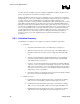
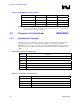
Figure 2-8. Overshoot and Undershoot during Dynamic VID Validation
Vcc
Time (µs)
1.6V
1.6V
0.8375V
0.8375V
Vcc
Time (µs)
Transition From Max To Min VID
Transition From Min To Max VID
Limit undershoot of DC
transition to 5mV
Must be compliant to
overshoot specifications