
Voltage Regulator-Down (VRD) 10.1 Design Guide


Processor Vcc Requirements
R
34 Design Guide
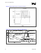
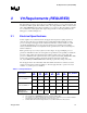
Overshoot Duration Analysis
TOS = Final Crossing of Vzc – Initial Crossing of Vzc
TOS = 35
µs – 15 µs = 20 µs < 25 µs = TOS_MAX
Time duration test passed
Amplitude and Time Duration Tests Passed => Overshoot specification is satisfied
2.8 VRD Output Filter (REQUIRED)
Desktop processor voltage regulators include an output filter consisting of large bulk decoupling
capacitors to compensate for large transient voltage swings and small value ceramic capacitors to
provide high frequency decoupling. This filter must be designed to stay within load line
specifications (Table 2-3 — Table 2-4 and Figure 2-1—Figure 2-2 ) across tolerances due to age
degradation, manufacturing variation, and temperature drift.
2.8.1 Bulk Decoupling
Bulk decoupling is necessary to maintain Vcc within load line limits prior to the VRD controller
response. Design analysis shows that bulk decoupling greatly depends on number of VRD phases,
the FET switching frequency. Design analysis determined that the most cost efficient filter
solution incorporates bulk capacitors with low (5 m
Ω) average ESR.
The D-VID mode of operation is directly impacted by the choice of bulk capacitors and output
inductor value in the VRD output filter. It is necessary to minimize Vcc settling time during D-
VID operation to hasten the speed of core temperature reduction. The speed of recovery is
directly related to the RCL time constant of the output filter. To ensure an adequate thermal
recovery time, it is recommended to design the output filter with a minimal output inductor value
and a minimal amount of bulk capacitance with minimum ESR, while providing a sufficient
amount of decoupling to maintain load line and ripple requirements. At this time, high-density
aluminum poly capacitors with 5 m
Ω average ESR have been identified as the preferred solution.
Failure to satisfy the Vcc settling time requirements defined in section 2.6 may invalidate
processor thermal modes; this may require a processor cooling solution (fan-heatsink) that is more
robust than recommended.
It is common for a motherboard to support processors that require different VRD configurations
(see Table 2-1). In this case, the Vcc regulator design must meet the specifications of all
processors supported by that board. This requires the VRD to adopt an output filter design that
satisfies the lowest socket load line value of all supported processors. For example, if a
motherboard is to support processors requiring 775_VR_CONFIG_04A with a 1.4 m
Ω socket
load line slope and 775_VR_CONFIG_04B requiring a 1.0 mOhm socket load line slope, the
VRD output filter must have a transient socket load line value of 1.0 mOhms to satisfy the noise
requirements of each processor.
Consult the appropriate platform design guideline for an output filter design capable of satisfying
load line and D-VID constraints.