
Voltage Regulator-Down (VRD) 10.1 Design Guide

Power Sequencing (REQUIRED)
R
Design Guide
41
4 Power Sequencing (REQUIRED)
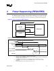
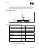
The VRD must correctly sequence power in accordance with Intel processor requirements. Figure
4-1 is a block diagram of the VRD connectivity with necessary signals and relevant power rails.
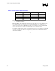
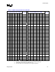
Figure 4-2.provides the timing protocol for these signals and power rails in LGA775 platforms.
Figure 4-1. Power-on Sequencing Block Diagram
Vtt VR
Vcc VR
Processor
Vtt
VTTPWRGD
Vcc
VID[5:0]
Output Enable
Vcc_PWRGD
Figure 4-2. Power Sequence Timing Diagram
Vtt
VTTPWRGD
VID[5:0]
Vcc
Vcc_PWRGD
T
D1
VID INVALID VID INVALIDVID VALID
T
D3
T
D4
VID[5:0]
Output Enable
T
OFF
T
OFF
NOTES:
1. Vtt comes up at the application of system power to the Vtt VRD.
2. Vtt VRD generates VTTPWRGD to latch the processor’s VID outputs and enable Vcc VRD, after the
Vtt supply is valid. See Section 9.2.
3. Vcc_PWRGD is generated by the Vcc VRD and may be used elsewhere in the system.
4. VTTPWRGD may also be referenced as VIDPWRGD. Table 4-1. Power Sequence Timing
Parameters
5. All power supply rails must be in regulator at the start of T
D4