
Voltage Regulator-Down (VRD) 10.1 Design Guide

Control Inputs
R
Design Guide
45
6 Control Inputs
6.1 Vcc Output Enable (REQUIRED)
The VRD must include an input signal to enable the Vcc output. When disabled, the VRD output
should be in a high-impedance state and should not source current. Once the VRD is operating
after power-up, it should respond to a de-asserted output enable by turning off Vcc power within
500 ms. Consult Section 4 for Vcc power sequence information. When Output Enable is pulled
low during the shutdown process, the VRD output must not exceed its previous voltage level
regardless of the VID setting during the shutdown process. Voltage below –100 mV is not
permitted at the output of the VRD.
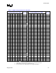
Table 6-1. Output Enable Specifications
Design Parameter Minimum Typical Maximum
Pull-Up Voltage Range Vtt
1
Pull-Up Resistor 620 Ω
2
680 Ω 750 Ω
3
V
IH
0.8 V -
V
IL
- 0.3 V
NOTES:
1. Consult Table 3-1 for Vtt specifications.
2. Value represents minimum resistance at tolerance limits.
3. Value represents maximum resistance at tolerance limits.
4. Voltage Identification (VID [5:0]) (REQUIRED)
The VRD must accept a six-bit code transmitted by the processor to establish the reference Vcc
operating voltage as defined by Table 9-1.
While operating in the D-VID mode, Intel processors can transmit VID codes across the six bit
bus with a 5
µs data transmission rate. To properly design this bus against timing and signal
integrity requirements (Table 6-3), the following information is provided. The VID buffer circuit
varies with processor generation and can be an open-drain or push-pull CMOS circuit
configuration. The VID bus must be designed to be compatible with each circuit; therefore a pull-
up resistor is required to bias the open drain configuration. The worst-case settling time
requirement for code transmission at each load is 400 nanoseconds, including line-to-line skew.
VRD controller VID inputs should contain circuitry to detect a change and prevent false tripping
or latching of VID codes during this 400-nanosecond window.
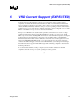
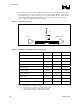
Intel recommends use of the D-VID bus topology described in Figure 6-1 and Table 6-3. Under
these conditions, traces can be routed with microstrip, stripline, or a combination with a maximum
of Four-Layer transitions. The main trace length can vary between ½ inch and 15 inches with a
maximum recommended line to line skew of 1 inch. The 680
Ω ±10% pull-up resistor can be
placed at any location on the trace with a maximum stub length of 1 inch.