
Voltage Regulator-Down (VRD) 10.1 Design Guide


Control Inputs
R
46 Design Guide
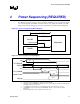
Some designs may require additional VID bus loads. In this case, care should be taken to design
the topology to avoid excessive undershoot and overshoot at each load. Failure to comply with
these limits may lead to component damage or cause premature failure. The responsible engineer
must identify minimum and maximum limits of each component and design a topology that
ensures voltages stay within these limits at all times.
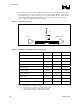
Figure 6-1. D-VID Bus Topology
Processor PWM Controller
R
TT
V
TT
L2
L1
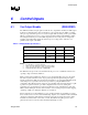
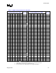
Table 6-2. VID Buffer and VID Bus Electrical Parameters
Design Parameter Minimum Typical Maximum
VID Bus Voltage - Vtt
1
-
Voltage Limits At Processor VID Lands - 0.100 - Vtt
2
V
IH
0.8 V - -
V
IL
- - 0.3 V
L
1
, VID trace length 0.5 inch - 15 inches
L
2
, Vtt Stub Length 0 inch - 1 inch
VID trace length skew - 1.0 inch -
VID trace width 5 mil - -
VID trace separation 5 mil - -
R
TT
, Pull-Up Resistor 620 Ω
3
680 Ω 750 Ω
4
NOTES:
1. Consult Table 3-1 for Vtt specifications.
2. Consult the processor datasheet for signal overshoot limits.
3. Value represents minimum resistance at tolerance limits.
4. Value represents maximum resistance at tolerance limits.