
Voltage Regulator-Down (VRD) 10.1 Design Guide

Output Indicators
R
Design Guide
53
9 Output Indicators
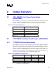
9.1 VCC_PWRGD: Vcc Power Good Output
(PROPOSED)
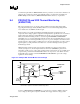
The Vcc VRD is to provide a power-good signal, which satisfies timing requirements defined in
section 4. The signal must remain asserted when the VRD is operating, except for fault or
shutdown conditions. Vcc_PWRGD must not be de-asserted during the D-VID operation.
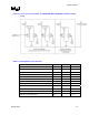
Table 9-1. Power Good Specifications
Design Parameter Specification
Signal Type Open-collector or equivalent
Voltage Range 5.5 V (maximum) in open state
Minimum IOL 4 mA
Maximum VOL 0.4 V
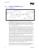
9.2 VTTPWRGD: Vtt Power Good Output (REQUIRED)
9.2.1 VTTPWRGD Electrical Specifications
The Vtt VRD is to provide a power-good signal to the processor and Vcc VRD, which satisfies
timing requirements defined in Section 4 and electrical conditions defined in Table 9-2. The
signal is to be asserted when Vtt reaches regulation and de-asserted after falling below tolerance
limits. This signal is to remain asserted when the Vtt VRD is operating, except for fault or
shutdown conditions. VTT_PWRGD must not be de-asserted during the D-VID operation. Each
buffer attached to this signal must satisfy input Vil and Vih conditions defined in Table 9-2. See
Section 6.1 for further information on the Vcc VRD Output Enable input.
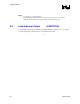
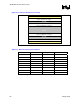
Table 9-2. VTT_PWRGD Electrical Parameters
Parameter Minimum Typical Maximum
Pull-up voltage - Vtt
1
-
Receiver Vih 0.8 V - -
Receiver Vil - - 0.3 V
Rise time (10% - 90%) - - 150 ns
NOTES:
1. Consult Table 3-1 for Vtt specifications