
Voltage Regulator-Down (VRD) 10.1 Design Guide

Output Indicators
R
54 Design Guide
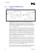
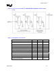
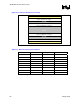
9.3 Example VTTPWRGD Circuit
Figure 9-1. VTTPWRGD Circuit
The circuit in Figure 9-1 satisfies the power sequence and rise time requirements of the
VTTPWRGD signal as defined in Section 4 and 9.2.1. The circuit consists of two functional
blocks. The first circuit block is centered around transistors A and B, which detect the Vtt
threshold and triggers the VTTPWRGD signal. The second block consists of transistors D and C,
which establish the necessary rise time and signal polarity. For this circuit, switching transistors
are selected. As a result, the transistors are either cut-off or in full saturation. For the following
discussion, please reference Figure 9-1.
At power-on, VTTPWRGD is tied low through the 2.2 k
Ω transistor with transistor D OFF. For
the benefit of the designer, the following passage describes the state of the circuit prior to Vtt
regulation. At start-up, transistor A will be OFF since Vtt is below the base bias threshold. This
establishes 0.7 V at the base of transistor B through the 10 k resistor tied to the 3.3 V stand-by. In
this configuration, transistor B is in saturation and the collector voltage is below the base bias
requirements of transistor C. As a result, Transistor C is OFF setting the collector of transistor C
and base of transistor D to the 3.3 V standby voltage. Transistor D is a PNP with the emitter
voltage tied to Vtt. With 3.3 V on the collector, transistor D is biased OFF in this configuration.
This forces VTTPWRGD to ground through the 2.2 k
Ω resistor. The 3.3 V supply provides a
strong reference to avoid false triggering of this signal, however the 5 V standby can also be used.
The 3.3 V standby supply was chosen for ease of routing.
Triggering of the VTTPWRGD signal occurs when the Vtt supply reaches regulation. The signal
is toggled approximately 2.5 ms after the 90% Vtt threshold is reached. This functionality is
established with an RC circuit connected to the base of transistor A. As Vtt rises to regulation, the
RC network (the 2.74 k
Ω resistor, 22.1 kΩ resistor, and 1.0 µF capacitor) will raise the base of
transistor A to 0.7 V. This causes transistor A to conduct, thereby removing the base bias of
transistor B. Removal of the base bias causes transistor B to switch off. This establishes a 0.7 V
base bias for transistor C through the 10 k
Ω resistor. With the existing collector bias, transistor C
will switch-on. This collector voltage, connected to the base of transistor D, is sufficient to
switch-on transistor D, thereby connecting VTTPWRGD to VTT.
This clever transistor network provides a low cost method of satisfying the VTTPWRGD trigger
and rise-time specifications. General purpose switching NPN and PNP are chosen for design
flexibility. Transistors A and B are contained in a single, 6-pin SOT-23 package; the