
Voltage Regulator-Down (VRD) 10.1 Design Guide

Output Indicators
R
56 Design Guide
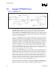
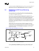
positive comparator terminal). As the thermistor temperature increases due to system loading, the
resistance will decrease. When the voltage drop across the thermistor falls below the trigger
reference voltage, established by R1 and R2, the comparator will change state and bias the bipolar
transistors. When biased, Q1 and Q2 provide the active low assertion of PROCHOT# and
FORCEPR# compliant to Table 7 signaling specifications. Q1 and Q2 must be selected to
adequately drive PROCHOT# and FORCEPR# VOL signaling values.
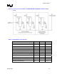
FORCEPR# is a processor signal with active-low input buffers terminated to the system Vtt (FSB
termination voltage). PROCHOT# is a processor signal that can be configured as i/o using open-
drain, output buffers terminated to the system Vtt (FSB termination voltage); This signal drives
and receives with active low signaling. In some processor configurations, this buffer is configured
as an output only signal To maintain reliable signaling, the bipolar transistor must be selected to
operate with a collector bias established by motherboard, processor, or chipset on-die termination
(See Figure 9-2). The bipolar transistors must be chosen to drive an the Vol levels identified in
Table 9-3 with an effective termination range defined in Table 9-3. Note that the termination
topology can take multiple forms; A generic representation is provided in Figure 9-3.
PROCHOT# and FORCEPR# may see this full configuration, or a subset including any
combination of the identified loads.
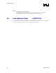
The values for R1, R2 and R3 in Figure 4 are included as an example and must be calculated
using specific design parameters. The value of R2 is adjusted to calibrate the comparator’s trigger
reference voltage (and assertion of the output signals) against the sensor voltage representing a
thermal violation.