
Voltage Regulator-Down (VRD) 10.1 Design Guide
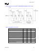

Output Indicators
R
58 Design Guide
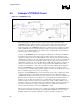
NOTES:
1. Consult Table 3-1 for Vtt specifications.
2. Bias for Q1and Q2 in the thermal monitor circuit is provided by the processor and chipset.
Additional termination must not be integrated into the thermal monitoring circuit.
9.5 Load Indicator Output (EXPECTED)
To assist VRD circuit debug and validation, the PWM controller supplier may choose to include
an output voltage that is a defined function of the VRD output current.
§