
Voltage Regulator-Down (VRD) 10.1 Design Guide


Motherboard Power Plane Layout
R
Design Guide
59
10 Motherboard Power Plane Layout
The motherboard layer stack-up must be designed to ensure robust, noise-free power delivery to
the processor. Failure to minimize and balance power plane resistance may result in non-
compliance to the die load line specification. A poorly planned stack-up or excessive holes in the
power planes may increase system inductance and generate oscillation on the rail at the processor.
Both of these types of design errors can lead to processor failure and must be avoided by careful
Vcc and Vss plane layout and stack-up. The types of noise introduced by these errors may not be
immediately observed on the processor power lands or during system-board voltage transient
validation, so issues must be resolved by design, prior to layout, to avoid unexpected failures.
Following basic layout rules can help avoid excessive power plane noise. All motherboard layers
in the area surrounding the processor socket should be used for Vcc power delivery; copper
shapes that encompass the power delivery region of the processor land field are required. A
careful motherboard design will help ensure a well-functioning system that minimizes the noise
profile at the processor die. The following subsections provide further guidance.
10.1 Minimize Power Path DC Resistance (EXPECTED)
Power path resistance can be minimized by ensuring that the copper layout area is balanced
between Vcc and Vss planes. A good Four-Layer board design will have two Vcc layers and two
Vss layers. Because there is generally more Vss copper in the motherboard stack-up, care should
be taken to maximize the copper in Vcc floods. This includes care to minimize unnecessary plane
splits and holes when locating through hole components, vias, and connection pads.
10.2 Minimize Power Delivery Inductance (EXPECTED)
At higher frequencies the ordering of the motherboard layers becomes critical as it is Vcc/Vss
plane pairs
which carry current and determine power plane inductance. The layer stack-up should
maximize adjacent (layer-to-layer) planes at a minimized spacing to achieve the smallest possible
inductance. Care must be taken to minimize unnecessary plane splits and holes when locating
through-hole components, vias, and connection pads. Minimized inductance will ensure that the
board does not develop low frequency noise which may cause the processor to fail (load line
violation).
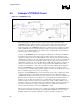
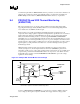
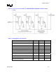
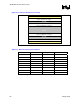
10.3 Four-Layer Boards (EXPECTED)
A well-designed 4-layer board will feature generous Vcc shapes on the outer layers and large Vss
shapes on the inner layers. The Vss-reference requirements for the front side bus are best
accommodated with this layer ordering. The power plane area should be maximized and cut-out
areas should be carefully placed to minimize parasitic resistance and inductance. Examples power
plane layout of Intel’s reference board are provided in Table 11-1 and Figure 10-1 to Figure 10-5.