
Voltage Regulator-Down (VRD) 10.1 Design Guide
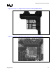
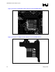
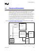
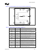

Motherboard Power Plane Layout
R
Design Guide
63
10.4 Six-Layer Boards (EXPECTED)
Six layer boards provide layout engineers with greater design flexibility compared to the Four-
Layer standard. Adjacent plane pairs of the same potential are not useful at higher frequencies, so
the best approach is to maximize adjacent, closely spaced Vcc/Vss plane pairs. The plane pair
separated by the PCB core material is of lesser importance since it is generally an order of
magnitude larger in spacing than other plane pairs in the stack-up. Because the Vss planes are
typically full floods of copper, an example of a well-designed 6-layer stack-up will have four Vcc
layers and two layers for Vss. The DC resistive requirements (section 10.1) of the power delivery
loop can still be met because the Vss floods are larger than the Vcc floods, and the higher
frequency needs are considered as there are four Vcc/Vss plane pairs to deliver current and reduce
inductance.
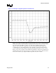
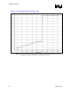
10.5 Resonance Suppression (EXPECTED)
Vcc power delivery designs can be susceptible to resonance phenomena capable of creating droop
amplitudes in violation of load line specifications. This is due to the interleaved levels of
inductively-separated decoupling capacitance. Furthermore, these resonances may not be
detected through standard VTT validation and require engineering analysis to identify and
resolve. If not identified and corrected in the design process, these resonant phenomena may yield
droop amplitudes in violation of load line specifications by superimposing with standard VRD
droop behavior. Frequency-dependent power delivery network impedance simulations and
validation are strongly recommended to identify and resolve power delivery resonances before
board are actually built. Careful modeling and validation can help to avoid voltage violations
responsible for data corruption, system lock-up, or system ‘blue-screening’
§