
Voltage Regulator-Down (VRD) 10.1 Design Guide


Electrical Simulation
R
Design Guide
65
11 Electrical Simulation
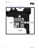
The following electrical models are enclosed to assist with VRD design analysis and component
evaluation for load line compliance. The block diagram shown in Figure 11-1 is a simplified
representation of the Vcc power delivery network of the Intel four-layer reference board
interfaced with the LGA775 socket. The board model, detailed in Figure 11-4, characterizes the
power plane layout of Figure 10-2 to Figure 10-5. The socket, detailed in Figure 11-6, models the
LGA775 electrical parasitics; it also provides a current load step model for exploring the system
droop response. The multiphase buck regulator and capacitor models should be obtained from
each selected vendor. When fully integrated into electrical simulation software, this model can be
used to evaluate PWM controller, capacitor, and inductor performance against the load line and
tolerance band requirements detailed in Section 2.2. To obtain accurate results, it is strongly
recommended to create and use a custom model that represents the specific board design, PWM
controller, and passive components that are under evaluation.
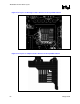
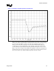
Figure 11-1. Simplified Block Diagram Representing Electrical Connectivity for the VRD on
the Four-Layer Intel Reference Motherboard
N6
N4
N2
N1
N5
East Phase Inductors
North Phase Inductors
Error Amplifier Input
Output: North Phases
Output: East Phases
C1
North
Bulk
Caps
C3
East
Bulk
Caps
C2
High
Frequency
Filtering
Capacitance
Multi-Phase Buck
Regulator
N2
N4
N6
Socket
N3
Motherboard
NOTE: Consult Figure 10-2 to Figure 10-5 for reference layout.