
Voltage Regulator-Down (VRD) 10.1 Design Guide


Electrical Simulation
R
66 Design Guide
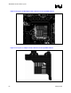
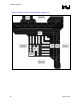
The motherboard model of Figure 11-4 represents the power delivery path of Intel’s reference
four-layer motherboard design. Input and output node locations are identified in Figure 11-5.
Feedback to the PWM controller error amplifier should be tied to node ‘N2’, the socket-
motherboard interface. Node ‘N1’ is the location where the ‘north’ phase inductors of the buck
regulator ties to the ‘north’ motherboard power plane. If the design incorporates more than one
‘north’ phase, the inductors of each should be tied to this node. ‘North’ bulk capacitors, C1, are
also connected to node ‘N1’. C1 represents the parallel combination of all capacitors and
capacitor parasitics at this location. Node ‘N5’ is the location where the output inductors of the
‘east’ side phases tie to the ‘east’ motherboard power plane. If the design incorporates more than
one ‘east’ phase, the inductors of each should be tied to this node. ‘East’ bulk capacitors, C3, are
also connected to ‘N5’. C3 represents the parallel combination of all capacitors and capacitor
parasitics at this location. Node ‘N3’ represents the socket cavity and is connected to the high
frequency filter, C2. C2 represents the parallel combination of all capacitors and capacitor
parasitics at this location.
Typical capacitor models are identified in Figure 11-6. Each model represents the parallel
combination of the local capacitor placement as identified in the previous paragraph.
Recommended parallel values of each parameter are identified in Table 11-2. Consult Section 2.8
for further details regarding bulk and high frequency capacitor selection.
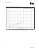
LGA775 electrical models are provided in Figure 11-7. The LGA775 socket is characterized by
three impedance paths that connect to the motherboard at ‘N2’ (‘north’ connection), ‘N4’ (‘south’
cavity connection), and ‘N6’ (‘east’ connection). Current is fed to this branch network through
the VTT Tool parasitic impedance (RVTT1, LVTT1, RVTT2, LVTT2), which is driven by
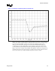
current source I_PWL. I_PWL is a piece-wise linear current step that is used to stimulate the
voltage droop as seen at the motherboard-socket interface and is defined in Figure 11-8 and Table
11-4. This load step approximates the low frequency current spectrum that is necessary to
evaluate bulk capacitor and PWM controller performance. It does not provide high frequency
content to excite package noise. The cavity capacitor solution, C2, is used as a reference for
designing processor packaging material and should not be modified except to reduce ESR/ESL or
increase total capacitance.
Caution: Failure to observe this recommendation may make the motherboard incompatible with some
processor designs.
The primary purpose of the simulation model is to identify options in supporting the socket load
line specification. Evaluation of the full power-path model will allow the designer to perform
what-if analysis to determine the cost optimal capacitor and PWM controller configuration. This
is especially useful in determining the capacitor configuration that can support load line
specifications across variation such as manufacturing tolerance, age degradation, and thermal
drift. The designer is encouraged to evaluate different bulk capacitor configurations and PWM
controller designs. However, the designer should be aware that the feedback compensation
network of most PWM controllers requires modification when the capacitor solution changes.
Consult the PWM controller datasheet for further information.