
Voltage Regulator-Down (VRD) 10.1 Design Guide

Electrical Simulation
R
Design Guide
69
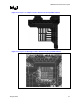
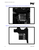
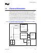
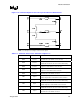
Figure 11-4. Schematic Diagram for the Four-Layer Intel Reference Motherboard
NOTE: Consult Figure 10-2 to Figure 10-5 for reference layout.
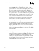
Table 11-1. Parameter Values for the Schematic of Figure 11-4
Parameter Value Comments
RMB1 0.93 mΩ
‘North’ power plane parasitic resistance from the buck regulator
output inductor to the LGA775 socket connection.
RMB2 0.85 mΩ
Power plane parasitic resistance from ‘north’ LGA775
motherboard connection to the center of the LGA775 cavity.
RMB3 0.70 mΩ
Power plane parasitic resistance from the center of the LGA775
cavity to the ‘south’ LGA775 socket connection.
RMB4 0.87 mΩ
Power plane parasitic resistance from the center of the LGA775
cavity to the ‘east’ LGA775 socket connection.
RMB5 0.97 mΩ
‘East’ power plane parasitic resistance from the buck regulator
output inductor to the LGA775 connection.
LMB1 104 pH
‘North’ power plane parasitic inductance from the buck
regulator output inductor to the LGA775 socket connection
LMB2 88 pH
Power plane parasitic inductance from ‘north’ LGA775
motherboard connection to the center of the LGA775 cavity.
LMB3 65 pH
Power plane parasitic inductance from the center of the
LGA775 cavity to the ‘south’ LGA775 socket connection.
LMB4 92 pH
Power plane parasitic inductance from ‘east’ LGA775
motherboard connection to the center of the LGA775 cavity.
LMB5 106 pH
‘East’ power plane parasitic inductance from the buck regulator
output inductor to the LGA775 connection.