
Voltage Regulator-Down (VRD) 10.1 Design Guide

Electrical Simulation
R
Design Guide
73
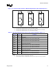
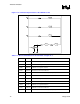
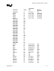
Figure 11-8.
Current Load Step Profile for I_PWL from the Schematic of
Figure 11-7
I
max
I
min
t
0
t
1
t
2
Time
Current (A)
I
max
I
min
t
0
t
1
t
2
Time
Current (A)
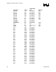
Table 11-4. I_PWL Current Parameters for Figure 11-7 and Figure 11-8
Parameter Value Comments
t
0
0 s Simulation ‘time zero’
t
1
250 µs
Time to initiate the current step. This parameter must be chosen at a time
that the Vcc rail is residin
g
at stead
y
state.
t
2
t
1
+ 1.25
µ
s
Time of maximum current
Istep 95 A Current step for load line testing
Imin 24 A Minimum current for simulation analysis
Imax 119 A Maximum current for simulation analysis
§