
Voltage Regulator-Down (VRD) 10.1 Design Guide


Appendix: LGA775 Version 1 Pinmap
R
Design Guide
91
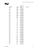
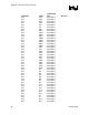
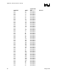
Land Name Land #
Signal Buffer
Type Direction
VSS T7 Power/Other
VSS U1 Power/Other
VSS U7 Power/Other
VSS V23 Power/Other
VSS V24 Power/Other
VSS V25 Power/Other
VSS V26 Power/Other
VSS V27 Power/Other
VSS V28 Power/Other
VSS V29 Power/Other
VSS V3 Power/Other
VSS V30 Power/Other
VSS V6 Power/Other
VSS V7 Power/Other
VSS W4 Power/Other
VSS W7 Power/Other
VSS Y2 Power/Other
VSS Y5 Power/Other
VSS Y7 Power/Other
VSS_MB_REGULATION AN6 Power/Other Output
VSS_SENSE AN4 Power/Other Output
VSSA B23 Power/Other
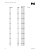
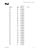
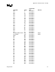
VTT A25 Power/Other
VTT A26 Power/Other
VTT A27 Power/Other
VTT A28 Power/Other
VTT A29 Power/Other
VTT A30 Power/Other
VTT B25 Power/Other
VTT B26 Power/Other
VTT B27 Power/Other
VTT B28 Power/Other
VTT B29 Power/Other
VTT B30 Power/Other
VTT C25 Power/Other
VTT C26 Power/Other
VTT C27 Power/Other
VTT C28 Power/Other
VTT C29 Power/Other
VTT C30 Power/Other
VTT D25 Power/Other
VTT D26 Power/Other
VTT D27 Power/Other
VTT D28 Power/Other
VTT D29 Power/Other
VTT D30 Power/Other