
VRM 9.0 DC-DC Converter Design Guidelines
VRM 9.0 DC-DC Converter Design Guidelines
16
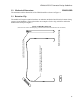
2.4 Alternate Module Dimensions
An optional module with the following features provide cost and thermal advantages in some
systems.
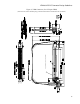
2.4.1 Dimensions
The dimensional option increases the maximum component thickness on the pin 1-31 side of the
module PCB from 0.25” to 0.50” (increases total module thickness from 0.576”, shown in Figure
3, to 0.826”).
2.4.2 Thermal capability
The intention of the greater thickness is to make room for heat sinking, accommodating higher
temperatures or lower airflow.
2.4.3 Capacitors
A further option places input and output filter capacitors on the system board instead of the
module. This puts the filtering on the load side of the VRM connector, opening up additional
heat sink space and reducing total component costs.
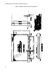
2.5 Heat Sink Connection
Heat sinks cannot be connected to any potential other than ground.
2.6 Board Temperature
To maintain the connector within its operating temperature, the VRM board temperature at the
connector interface must not exceed a temperature of 90°C within 2.54 mm (0.1”) from the top of
the connector. To meet the 90°C limit, a board constructed from 4-ounce cladding is
recommended.
The VRM board must interface with the connector through gold lands (fingers) that are
1.27 ± 0.05 mm (.050 ± .002”) wide by a minimum of 5.08 mm (.200”) long and spaced
2.54 ± 0.05 mm (.100 ± .002”) apart. Traces from the lands to the power plane should be a
minimum of 0.89 mm (.035”) wide and a minimal length.
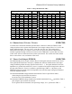
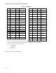
3 Tests and Standards
3.1 Environmental PROPOSED
Design, including materials, should be consistent with the manufacture of units that meet the
environmental reference points in Table 4.