
VRM 9.0 DC-DC Converter Design Guidelines

VRM 9.0 DC-DC Converter Design Guidelines
5
1 Electrical Specifications
1.1 Output Requirements
1.1.1 Voltage and Current REQUIRED
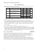
The VRM 9.0 Voltage Regulator Module is a DC-DC converter that supplies the required voltage
and current to a single processor as shown in Table 1. The maximum voltage is determined by
the five-bit VID code provided to the VRM, as described in Section 1.3.2. The specifications in
Table 1 are for the VRM only. The computer system board must supply additional decoupling
capacitance and sufficient plane area to carry the high DC currents. It is desirable that a single
model of the VRM be able to support all processor types, if this does not significantly affect
VRM cost and availability, so that field upgrades of processors will not require a new VRM.
1.1.2 Output Voltage Tolerance REQUIRED
The voltage measured at the VRM connector pins on the system board must be within the range
shown in Table 1, except during input voltage turn-on and turn-off. See Section 1.1.5 for
turn-on and turn-off tolerance.
Voltage tolerance includes:
− Initial DC output voltage set-point error
− Component aging effects
− Output ripple and noise
− Full ambient temperature range and warm up specified in Section 3.1.
− Both static operation and dynamic output load changes from minimum-to-maximum or
maximum-to-minimum loads specified in the tables above.
Output voltage tolerances increase with output current levels to compensate for the increasing
voltage drops in the power distribution path. Table 1 shows the relationship of V
CC_CORE
(measured at the processor pins) and I
CC
for different processors.
1.1.3 No Load Operation EXPECTED
The VRM should operate in a no-load condition: i.e., with no processor installed. The VRM
does not need to meet the output regulation specifications described in Table 1, but its output
must not exceed 110% of the value of the maximum DC output voltage, and it must not trigger
over-voltage fault detection circuitry. When the VRM is subsequently loaded with the minimum
values listed in Table 1, it must begin to regulate and source current without triggering failures or
causing control signal malfunction.
1.1.4 Turn-on Response Time PROPOSED
The output voltage should reach its specified range within 50 msec of the input power reaching
its minimum voltage.
1.1.5 Overshoot at Turn-On or Turn-Off REQUIRED
Overshoot upon the application or removal of the input voltage must be less than 2% above the
nominal output voltage set by the Voltage Identification (VID) code. No negative voltage may
be present on any output during turn-on or turn-off.