
VRM 9.0 DC-DC Converter Design Guidelines


VRM 9.0 DC-DC Converter Design Guidelines
6
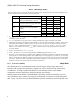
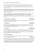
Table 1, VRM Output Ratings
Note: This table shows processor specifications for reference only. Please refer to the processor specifications in
the latest Intel
®
Xeon™ or Pentium
®
4 processor data sheet.
Symbol Parameter VID Minimum Maximum
Unit
1.70 1.609 1.70
Vout-VRM
Output voltage measured at the solder
side of the VRM mating connector
1,2,3
1.50 1.408 1.50
V
1.70 1.560 1.70
V
CC_CORE
Output voltage measured at the
processor sense pins on the solder side
of the processor socket
1,2,3
1.50 1.330 1.50
V
1.70
2.1
V
MAX
Maximum, non-operating (failure)
voltage
1.50
1.75
V
1.70 60
Iout
MAX
Maximum static VRM current for
Vout
4,5
1.50 65
A
dIout/dt
MAX
Output slew rate
6
50
A/µs
1. V
CC_CORE
–minimum at Iout
MAX
below. For V
CC_CORE
–minimum at other loads, please refer to specifications in
the latest processor data sheet.
2. V
CC_CORE
-maximum is set by the processor’s Voltage Identification (VID) code inputs to the VRM.
3. Maximum (VID setting) and minimum output voltages are for both static and transient conditions. Intel’s power
distribution model assumes a VRM set-point accuracy of 0.8%. The processor should not be subjected to any
static V
CC
and I
CC
combination wherein V
CC
exceeds (V
CC-MAX
+ V
CC-MIN
)/2 + 0.055·(1 – I
CC
/I
CC-MAX
) (volts).
Moreover, Vcc should never exceed V
CC-MAX
(VID). Failure to adhere to this specification can shorten the
processor lifetime.
4. Iout
MAX
is measured at (V
CC-MAX
+ V
CC-MIN
)/2.
5. Iout
MAX
allows for a 10% current-sharing imbalance in FMB applications (Section 1.1.7).
6. dIout/dt
MAX
is the output slew rate capability of the VRM for a minimum-to-maximum or maximum-to-minimum
load step with no external load capacitance at the VRM output, for testing purposes. In actual use, it is expected
that the system board has sufficient capacitive decoupling to slow the processor slew rate to 50A/µS at the VRM
output pins. When the module is specified to require output capacitance on the system board (e.g., in the option
proposed in Section 2.4), the test load must include the capacitance.
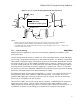
1.1.6 Converter Stability REQUIRED
The VRM needs to be unconditionally stable under all output voltage ranges and current
transients with system board capacitance ranging from 0 µF to 20,000 µF and with less than
2.0 mΩ ESR. A voltage regulator imbedded on a system board needs to meet stability
requirements with the output filter capacitance design on that board.
Stability requirements include a Thermal Monitor operating condition in which the processor
may periodically stop to reduce its average power dissipation in response to a high-temperature
alert. Figure 1 shows worst-case Thermal Monitor operation (maximum current in the ON state).