
VRM 9.0 DC-DC Converter Design Guidelines


VRM 9.0 DC-DC Converter Design Guidelines
9
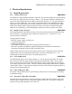
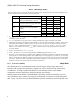
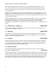
Table 2, Voltage Identification (VID)
Processor Pins (0 = low, 1 = high) Vcc Processor Pins (0 = low, 1 = high) Vcc
VID4 VID3 VID2 VID1 VID0 (VDC) VID4 VID3 VID2 VID1 VID0 (VDC)
1 1 1 1 1 Of
f
0111 1 1.475
1 1 1 1 0 1.1 0111 0 1.5
1 1 1 0 1 1.125 0110 1 1.525
1 1 1 0 0 1.15 0110 0 1.55
1 1 0 1 1 1.175 0101 1 1.575
1 1 0 1 0 1.2 0101 0 1.6
1 1 0 0 1 1.225 0100 1 1.625
1 1 0 0 0 1.250 0100 0 1.65
1 0 1 1 1 1.275 0011 1 1.675
1 0 1 1 0 1.3 0011 0 1.7
1 0 1 0 1 1.325 0010 1 1.725
1 0 1 0 0 1.35 0010 0 1.75
1 0 0 1 1 1.375 0001 1 1.775
1 0 0 1 0 1.4 0001 0 1.8
1 0 0 0 1 1.425 0000 1 1.825
1 0 0 0 0 1.45 0000 0 1.85
1.4 Remote Sense (VO-sen+, VO-sen–) EXPECTED
A remote sense connection should be provided at the connector to allow the VRM to sense
voltage elsewhere in the system and compensate for an output voltage offset of ≤ 55 mV in the
power distribution path. VO-sen+ is the + sense line, and VO–sen– is the sense return.
Differential sense inputs are required. In the event of an open sense line the VRM should
maintain regulation through a local sense resistor on the VRM board. Systems that do not use
remote sense will not connect these lines on the system board. The remote sense lines should
draw no more than 1 mA, to minimize offset errors.
1.5 Power Good Output (PWRGD) EXPECTED
The VRM should provide an open collector Power Good signal consistent with TTL DC levels.
This signal should transition to the open (>100kΩ) state within 10 milliseconds of the output
voltage stabilizing within the range specified in Section 1.1.1. The signal should be in the low-
impedance (to ground) state whenever Vout
VRM
is outside of the required range below and be in
the open state whenever Vout
VRM
is within its specified range (Table 1). On power up, the
PWRGD signal must remain in the low-impedance state until the output voltage has stabilized
within the required tolerance.
The minimum PWRGD voltage should be the minimum Vout
VRM
specified in Table 1,
minus margin to prevent false de-assertion,
but at least 95% of the minimum Vout
VRM
.
The maximum PWRGD voltage should be the nominal (maximum)Vout
VRM
specified in Table 1,
plus margin to prevent false de-assertion,
but no greater than the maximum, non-operating voltage, V
MAX
, specified in Table 1.